Epitaxial growth of thin films[1][2][3] on a substrate of the same atomic species is considered homoepitaxy, such as Si atoms deposited on a Si substrate (Fig. 1.5a). The interface of a homoepitaxially formed structure is considered the homojunction of the material. Generally, a homojunction is similar to the bulk lattice of the material and is ideally indistinguishable from the bulk structure.
Figure 1.5: Homoepitaxy/Heteroepitaxy. a) Homoeptaxial interface. A homojunction is ideally indistinguishable from the bulk lattice. b) Heteroepitaxial interface. A heterojunction between dissimilar materials forms dislocations due to lattice spacing mismatch. |
||||||
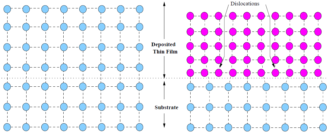
Heteroepitaxy refers to the process of epitaxial growth on a dissimilar substrate material, such as Al deposited on a Si substrate (Fig. 1.5b). A heteroepitaxially formed structure has a heterojunction at the interface of the two materials. The interface of a heterojunction generally induces a strain on the lattice of several planes of atoms in each material. The extent of heterojunction strain is typically related to mismatch between the atomic spacing of each material in order to form appropriate bonds with each other. In the current investigation, however, the amount of heterojunction strain between c-Al and c-Si is negligible since the Al layer is relaxed as a result of preconditioning the Si surface[4] by surface reconstruction. This will be explained in a subsequent chapter.
References
- , The Science and Engineering of Microelectronic Fabrication. Oxford University Press, 1996.
- , VLSI Technology. Bell Telephone Laboratory, Inc., 1983.
- , Electronic Thin Film Science for Electrical Engineers and Materials Scientists. Macmillan, 1992.
- , “Epitaxial growth of Al on Si by thermal evaporation in ultra-high vacuum: growth on Si(100)2x1 single and double domain surfaces at room temperature”, Surface Science, vol. 236, 1990.