The electrostatic properties of nanoscale systems differ from larger, meso- or macroscopic systems largely because of the total number of charges they may contain. This is largely because the system will undergo a process of dielectric breakdown in which the system of charges "explodes" in an abrupt discharge of charged particles.
For most systems, the charged particle of interest is the electron. The charge, movement, and electrostatic potential energy associated with electrons are important properties involved in micro- and nanoelectronics as found in almost all of today's electronic devices. Whether the nanoscale system is a single atom or the gate dielectric material in a single transistor, the system is spatially constrained in a way that larger systems are not. Consequently, a physical property like capacitance is determined differently from conventional (textbook) means.
The conventional (textbook) determination of capacitance is often modeled in terms of a parallel plate capacitor in which the field of electrostatic potential experienced by electrons in the system is globally defined by the shape of large thin metallic plates. However, in a nanoscale system such as a quantum dot, the electric potential typically is not uniformly distributed in space because the dielectric properties of nanoscale metal structures is different from their macroscopic counterparts. Additionally, in general, nanoscale systems function in the absence of any metallic structures. Even in large scale "computational" systems like the human brain, the functionality of the system is not governed by metallic structures, but by spatially varying contours of electric potential surfaces.
Quantum Treatment of Nanoscale Systems
In my doctoral research, I initially pursued a quantum mechanical framework I had proposed that considered "what if we treated the distribution of an electron's charge in accordance with its wavefunction?" By this, my doctoral advisor and I conceded that we (the scientific community) do not have an absolute agreement about what a wavefunction is. In most applications, the wavefunction can be viewed as part of the statistical distribution of a particle's physical properties in all space. This curiously means that there is no physical property represented by the wavefunction itself, but we can use this piece of mathematics to determine things like the probability distribution function across a region of space in which we would expect to find the particle (for example) with some probability when we measure or "look for" it. This work was unfortunately left incomplete because my advisor one day serendipitously interrupted my work at the point where I was just about to begin numerical calculations using my complete framework. Once I complete an online version of my doctoral thesis, you'll find more about this approach in chapter 5.
Classical Treatment of Nanoscale Systems
In the closing eight months of my doctoral research program in electrical engineering, I rapidly constructed a new electrostatics framework that may be best described as a "comprehensive electrostatics interactions framework" of charged particles suitable for nanoscale systems. The reason why I claim this framework to be comprehensive is that is a general formulation of the framework of stored electrostatic energy in systems with charges in the presence of dielectric materials. After review of several dozen textbooks on this specific subject, I determined that the textbook by Jackson is the best treatment for its completeness, though it is not complete. Instead, Jackson is the only author who appears to intentionally allude to the fact that there is an electrostatic interaction whose associated energy he sets to zero for convenience. Thus, Jackson implies that in general this interaction does in fact exist, but for the types of situations of interest to most textbook authors and physics students, the resulting interaction is negligible. The type of situations I'm referring to here are either cases in which the external charges sources of the electric field in which Jackson places the dielectric system to be evaluated is made of far more charges than the number of free charges in the system such as in a large metallic structure (in which case, the total number of charges is exceedingly large). It should come as no surprise that subsequent sections of Jackson's text take up the subject of metallic systems.
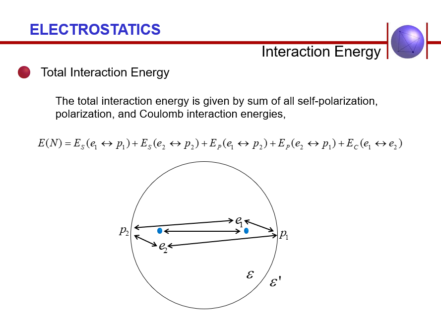
Alternatively, and similar in manner to my approach, if Jackson were to treat the case of electrostatic energy stored in a system of free charges and a dielectric object, this energy term would not be zero. From my framework, in fact, the fraction of the total energy stored in the system due to this electrostatic interaction term is as much as one-half, or fifty percent! Why? Because when the system contains a small number of charges, it's the distribution of those charges in space that give rise to complex electric potential surfaces and no longer very-well approximated by the shape of their metal container (cf. parallel plate capacitor).
Subsequently, this new body of research I've begun is a close look at the geometric symmetry properties of charged particles.
In my doctoral advisor's professional memoir, The World and I, he refers to this work as follows:
"Tim LaFave's dissertation led to a new branch of many body systems involving going far beyond a few electrons, into the domain similar to the Periodic Table of elements. For example, we can now start to understand the meaning of capacitance of nanoparticles. . . . What is most amazing is the fact that the Intra-phasic energy E(N-1,1e) - E(N) vs. number of electron is almost identical to the Periodic Table of elements!" [Raphael Tsu, The World and I, Litfire Publishing (March 8, 2018), ISBN-10: 1641515880 ]
Note: The labels we used at the time to describe each type of electrostatic interaction have changed. I made this change to be clear about the type of interaction as well as to avoid the potential for confusion with unrelated interaction types. Specifically, self-polarization has more recently been renamed "direct polarization" to avoid confusion with "self-interaction" or "self-energy" terms as appearing in my advisor's early 1990s paper. I want to carefully review this paper on my website to discuss this important difference as well as correct several typos and data errors that appeared in the original article. Unfortunately these errors were carried over to both of his books, Superlattice to Nanoelectronics (eds. 1 and 2). The other label change is from "polarization" to "indirect polarization" which refers uniquely to the interaction of a free charge with the electric potential formed by surface charge contributions due to other free charges (hence, "indirect").
A Scientific Discovery of the Classical Underpinnings of Atomic Structure
Among the theses I compiled for my doctoral dissertation is the discovery of a remarkable connection between the classical electrostatic energetics of electrons constrained to a sphere and the electron structure of atoms as distributed across the entire periodic table. To read more about this, have a look at "Correspondences between the Classical Electrostatic Thomson Problem and Atomic Electronic Structure". If you'd like a great summary of this work, have a look at this giant poster that includes a periodic table of electron energies within each N-electron system.
Below is the original slide of my dissertation presentation as I made my argument for abrupt changes in energy differences in each energy solution of the Thomson problem and the abrupt changes associated with the electron orbitals of "outermost" electrons in atomic structure as they appear throughout the periodic table. Of some interest, the partitioning of interaction energies in the graph by interaction type was an attempt to identify the source of these abrupt jumps. However, both the original interactions model and thinking about the source of such abrupt jumps has changed.
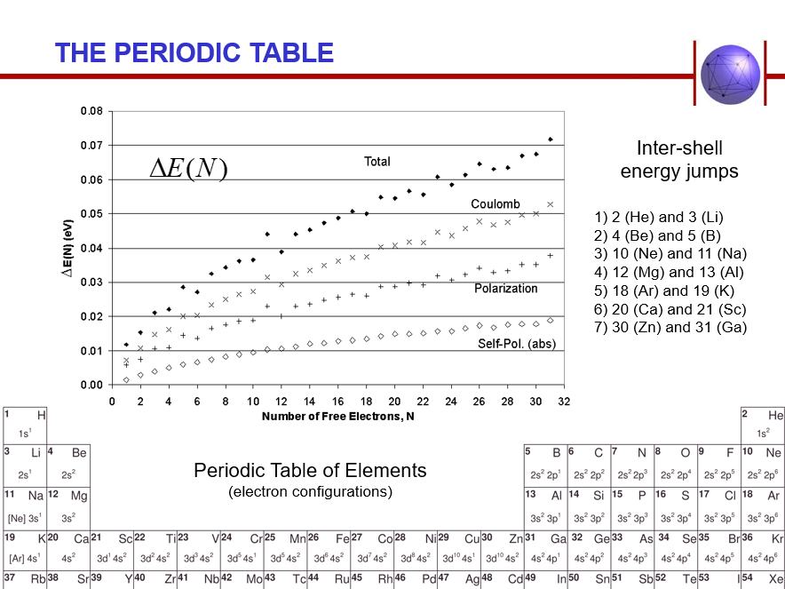
The premise of this discovery is remarkably independent of the size of the system. However, as noted in the paper linked above, if we treat the Thomson Problem within a dielectric sphere (as I had done in my seminal work on the classical treatment of electrons in a spherical quantum dot of silicon embedded in a uniform region of silicon dioxide) the corresponding features are greatly enhanced. One of the most remarkable features, in my opinion, is that the geometric symmetry properties found in the single-shell of electrons in the Thomson problem yield correspondences with the multi-shell system of real atoms. One may make some speculative hypotheses here to include:
- The angular electrostatic locations of inner shell electrons "fill-in" the angular vacancies of the outer shell with varying percentage of charge.
- The single-shell Thomson problem solutions are the configurations toward all electrons in any given atom are driven.
As I do not yet have a direct mathematical connection between the Thomson problem solutions and, for example, the spherical Bessel functions in the formal quantum mechanical formulation of atomic electron orbitals, I leave this conversation at this level of speculation for anyone interested in pursuing the matter further. However, be absolutely aware that no claim is made that these electrostatic configurations represent the actual locations of electrons in atomic systems. I merely posit that these geometric solutions are the spatial configurations toward which electrons in atoms are driven (by least energy principles) and that it's exceptionally unlikely they ever achieve.
Discrete Charge Dielectric Model of Electrostatic Energy
The comprehensive electrostatics interactions framework I devised as part of my treatment of electrons in a spherical quantum dot includes an energy term as I noted above is the mathematical equivalent of Jackson's energy term associated with external source charges. For the interested reader, the undergraduate textbook by Griffiths introduces a mathematically equivalent term in the form of a "spring energy" term that appears to have been invented such that the resulting total energy expression is equivalent to Jackson's (as has been shown in a great American Journal of Physics article by Das). The name of my framework was something my advisor spent considerable time worrying about. One day he excitedly suggested it should be called the "Discrete Electronic Devices Model," but I not only realized that we already call all those little devices on printed circuit boards "discrete electronic devices," but the abbreviation of the model, "DED," would be read in a very-much undesirably way. I was quick with this latter argument because Ray was motivated by his friend's deliberations over the use of the abbreviation for charge-coupled devices, or CCDs as well as how he and Leo Esaki intended to call their new invention something like "manmade materials" since it was the very first time in human history that materials exhibiting two-dimensional properties was intentionally and controllably made. He had also explained that someone told him (perhaps the inventor of CCDs) that "manmade materials" wasn't sexy enough, so they eventually landed on the super-sexy name of superlattices.
I already had a name for my model in mind. One that would capture what I believed were the important and distinguishing features of the model: Discrete Charge Dielectric (DCD) model. The model is unique to cases where the discreteness of charges is important, that applies to any kind of charged particles, and when the dielectric properties of the system are important and not washed out by the presence of metallic structures.
For details, read "Discrete Charge Dielectric Model of Electrostatic Energy."
The Thomson Problem
For my suggested contribution to the as-yet unsolved general solution of the Thomson problem, read "Discrete Transformations in the Thomson Problem."
Nanoscale Capacitance
After Ray spent a month or so reviewing what I claimed to be a connection between the classical energetics of the Thomson problem and atomic electron structure, he shook my hand in congratulations for the discovery. This is when he slumped back in a small chair in my student office and grudgingly asked me to go another step further and formulate a new approach to the capacitance of few-electron nanoscale systems. I was furious for many reasons as I've discussed elsewhere -- mostly because I knew I had far more than enough to defend my dissertation (my dissertation includes at least four separate theses!) -- so I went home that Friday in quiet fury. I cracked open a new ream of printer paper and just poured all my thoughts down onto hundreds of blank pages. By Sunday evening I had a complete picture of nanoscale capacitance based on my DCD model for electrostatic energy, and in the working language Ray and I had devised, I condensed my framework for monophasic capacitance into a couple sheets of paper. That Monday morning, I quietly entered Ray's office. Set the two pages down on his desk while saying "here's capacitance" and then quietly walked back to my desk to get a little more sleep.
After several days of reviewing what I had written down, Ray came to me and explained how he arrived at his assumption of a half-potential for the single-electron capacitor as he wrote in his book Superlattice to Nanoelectronics. He assumed that the electron would experience the average of the total potential difference, but said he had no real rationale for making the assumption. He insisted his math in his book was absolutely sound but couldn't figure out why there was a factor of one-half difference between the capacitance of when the system was connected and when it was unconnected. I hadn't read his derivations, but when he explained this to me, my first question was whether his book described a single-electron system or not. It made immediate sense to me why there would be a one-half factor but only if it was a single-electron case. It turned out to be exactly the case. And so we discussed things at greater length and eventually published a few papers. One of which you can grab off ResearchGate for free: "Capacitance: A property of nanoscale materials based on the spatial symmetry of discrete electrons."