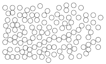
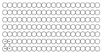
Semiconductor devices are generally fabricated by depositing thin films of atomic materials categorized by the degree to which atoms in the material are spatially ordered. An amorphous thin film (Fig. 1.3a) is a material in which atoms lack any coherent order. A crystalline thin film (Fig. 1.3b) is a material with periodic atomic order. Polycrystalline films (Fig. 1.3c) contain small regions, called grains, of crystalline material oriented differently with respect to each other. These three types of silicon material are referred to in their abbreviated forms such as "a-Si", "c-Si," and "p-Si," respectively.
Figure 1.2: Basic MOSFET Goals. a) The typical MOSFET has rather bulky features that consume device voltages and slow the device. b) With shallow source and drain regions, combined with a shortened gate length, the MOSFET becomes faster and consumes less power. |
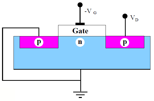
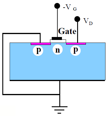
Figure 1.3: Three Types of Thin Films. a) Amorphous, with no apparent atomic order, b) crystalline, with either two- or three-dimensional periodicity of a conventional unit cell (dashed lines outline unit cell), and c) polycrystalline, consisting of several small grains of crystalline material. (Grain boundaries are indicated with bold lines.) |
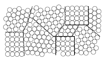
The crystallinity of a thin film usually refers to the three-dimensional order of a bulk material. A crystalline material may have two-dimensional atomic periodicity (herein referred to as diperiodicity) associated with its bounding surface and interfaces with other materials. An understanding of both bulk and surface periodicity are essential to the current investigation.
A crystal thin film is characterized by the periodic repetition of a unit cell throughout the three-dimensional arrangement of atoms in the conventional unit cell. Figure 1.4 indicates the various types of conventional unit cells relevant to the current investigation. There are only 14 possible Bravais lattices that can be repeated three-dimensionally[1][2]. The number of possible diperiodic unit cells, however, is infinite.
Figure 1.4: Bravais Lattices. Four of the fourteen possible Bravais lattices are shown. a) Simple cubic (conventional unit vectors shown, b) body-centered cubic (bcc) with a single atom at the body center of a simple cubic structure, c) face-centered cubic (fcc) with an atom at the center of each face of the simple cubic structure, and d) diamond, easily considered as the inclusion of four (dark) atoms in the fcc unit cell. The bonds of two atoms form the letter "M" diagonally across the bottom face of the diamond unit cell. The other two atoms bond in the shape of the letter "W" across the top plane, perpendicular to the "M." The location of these atoms is \(\frac{1}{4}\vec{a}_1, \frac{1}{4}\vec{a}_2, \frac{1}{4}\vec{a}_3\) from each of the brighter atoms. Thus, a diamond Bravais lattice may be considered as two interpenetrating fcc lattices. |
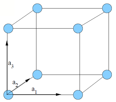
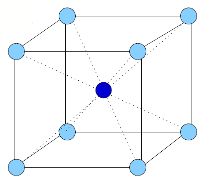

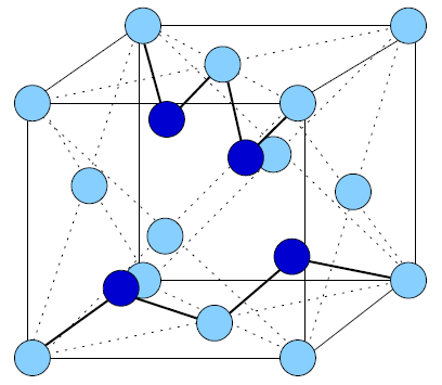
In the current investigation, crystalline Al forms a face-centered cubic (fcc) lattice (Fig. 1.4c), and crystalline Si forms a diamond lattice (Fig. 1.4d). In the cubic system, \(\left| a_1 \right| =\left| a_2 \right|=\left| a_3 \right|\). A diamond lattice is the combination of two interpenetrating fcc lattices of the same atomic species offset by \(\frac{1}{4}\vec{a}_1, \frac{1}{4}\vec{a}_2, \frac{1}{4}\vec{a}_3\) with respect to each other. The lattice dimensions of Al and Si are given in Table 1.1
|
Table 1.1: Dimensional Data of Al and Si[2].
|
References
- , “Solid State Physics”, Cornell University, 1976.
- , Introduction to Solid State Physics, 7th ed. Wiley, 1996.