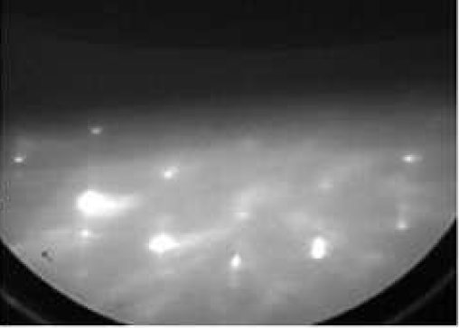
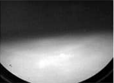
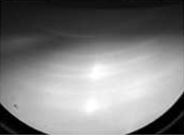
A Si(100) wafer is oxidized ($\theta_{\textrm{ox}}\sim1000$ Å) and patterned using BOE as previously outlined. The substrate is heated to 760°C for final cleaning, then cooled to room temperature. Initial RHEED, after cleaning to this temperature (Fig. 5-11a), indicates that the Si(100) surface remains unclean ($1\times 1$) as in the SMME Si(100) sample. Al is deposited ($T_{\textrm{Al}}=1140^\circ\textrm{C}$) at an operating pressure of $7\times 10^{-9}$ Torr for 90 minutes ($\sim2000$ Å). Immediately after Al deposition begins, a RHEED pattern (Fig. 5.11d) indicates p-Al deposition combined with the penetration of the c-Si substrate diffraction pattern. This indicates that the substrate surface is exposed to the electron beam. This behavior may indicate formation of Al islands on the Si surface due to the presence of residual oxide.
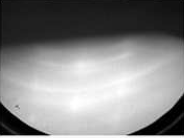
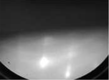
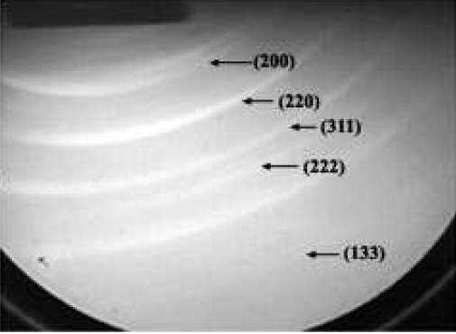
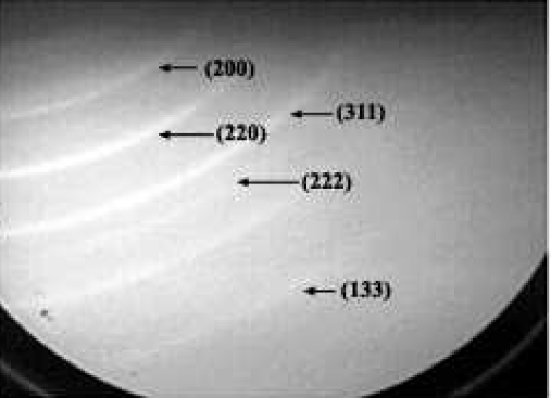
As the Al deposition proceeds (Fig. 5.11e,f), the Al becomes more and more crystalline, as previously recorded on the SMME Si(100) sample (measured ratio with respect to the Si pattern is 1.33 -- cf. 1.34 per standard values). This is due to the coalescence of islands and preferential growth of low-energy grains. However, as the substrate is heated to $360^\circ$C (Fig. 5.11g), the Al is observed to revert to a polycrystalline state ending with Fig. 5.11b possibly due to interaction with surface oxides. Si is then deposited from an electron beam evaporator source (9.5 KeV, 0.1 A) for 15 minutes leaving behind the fingerprint of p-Al (Fig. 5.11c), as expected.
|
|||||
| Figure 5.11. RHEED Investigation of SMM-SOI Si(100). a) Unreconstructed Si(100) diffraction pattern taken from a Si(100) wafer. b) Polycrystalline Al mediator (after deposition) and c) p-Al after deposition of Si diffusor (cf. Fig. 5.8) at $T_s=360^\circ\textrm{C}$. A closer inspection of the RHEED sequence during the deposition of Al indicates d) an initial combination of p-Al with c-Si transforming into e) stronger p-Al (rings). This may indicate the formation of Al islands in the seed area, exposing the Si substrate to the electron beam. The p-Al results after the deposition at room temperature. Once the substrate is heated to $T_s=360^\circ\textrm{C}$, the f) Al islands coalesce into an Al mediator film. As Si deposition ensues, g) the crystallinity of Al is lost to damage done by the Si, finally ending in p-Al in c.). | |||||