Here, SMME is utilized as a new silicon-on-insulator (SOI) fabrication technology. A Si(111) substrate is prepared with a 500 Å thick oxide pattern using a reactive ion etch (RIE) method.
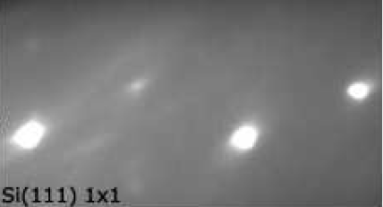
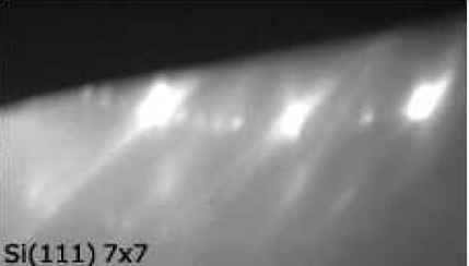
After insertion to the UHV MBE chamber and placement in the substrate holder, the unreconstructed Si(111) surface yields a relatively clean $1\times 1$ RHEED pattern (Fig. 5.8a). After final cleaning to $850^\circ \textrm{C}$ in vacuum, the Si(111) substrate is shown to be $7\times 7$ reconstructed (Fig. 5.8b). The RHEED image is a reciprocal representation of real-space crystal lattice dimensions. The diperiodic unit cell is therefore proportional to 1/7 of the $1\times 1$ RHEED pattern. Hence, there are seven divisions in the RHEED pattern between $1\times 1$ diffraction spots.
|
(a) (b) (c) (d) |
|
|
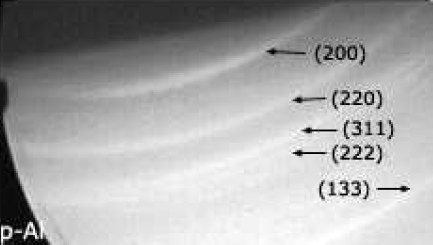
Figure 5.8. In Situ RHEED Analysis of SMM-SOI Sample. a) The unreconstructed $1\times 1$ Si(111) substrate. b) $7\times 7$ surface reconstruction of Si(111) after final cleaning by heating to $900^\circ\textrm{C}$. c) Diffraction after deposition of Al mediator thin film ($\sim 360$ Å). d) Diffraction from Al surface after Si diffusor deposition ($\sim650$ Å) shows a severely damaged Al mediator. |
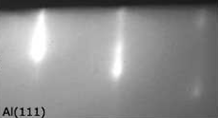
After deposition of the Al mediator at room temperature the RHEED pattern (Fig. 5.8c) indicates a 1.34 ratio of reciprocal Al lattice spacing to $1\times 1$ Si dimensions, as expected. Additionally, Fig. 5.8c demonstrates Al surface smoothness by the presence of vertical spikes. As expected, no Al islands form after the deposition of an Al mediator at room temperature.
|
|
|
| Figure 5.9. Cross Sectional SEM of SMM-SOI Si(111). Si ELO bridges are shown with smooth surfaces indicating the uniform overgrowth of a buried Si diffusor layer during SMM-SOI on Si(111). |
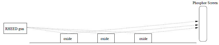
A feature of SMM-SOI observed by RHEED is the prevalent formation of polycrystalline Al after the deposition of Si diffusors (Fig. 5.8d). Provided this result, note the smooth, single-crystalline formation of Al indicated by Fig. 5.8c with no appearance of p-Al. This may be indicative of a single-crystalline overgrowth of Al on oxide. The RHEED beam sweeps across the substrate surface at a very shallow angle. Thus, the topmost peaks (over oxide) dominate the resulting RHEED pattern (Fig. 5.10). The change in the diffraction pattern from c-Al to p-Al after Si deposition is clearly due to a strong interaction of Si with Al. If the electron beam were incident on an off-oxide region, the RHEED patterns would have been similar to those of SMME on Si(111). Should the wafer surface have been contaminated during oxidation stages, the RHEED patterns would have been much more similar to the unreconstructed Si(100) surface during SMME (section 5.1.2).
|
|
|
| Figure 5.10. Shallow Angle of RHEED Beam. The electron beam produced by the RHEED gun is incident at a very shallow angle ($\lt2^\circ$). Thus, the uppermost part of the oxide pattern structure dominates the diffraction pattern produced on the phosphor screen. |
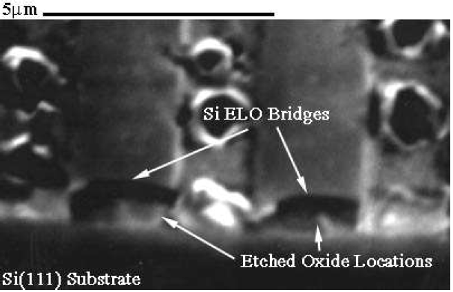
A cross sectional SEM investigation is performed that clearly indicates lateral overgrowth of the buried Si diffusor layer. The 2/2 $\mu$m region (cf. Fig. 4.2a) is prepared by cleaving the sample perpendicular to the length of the oxide strips. A small section of this cleaved sample is exposed to an HF solution that dissolves the underlying oxide from the cleaved edge, as well as most of the Al mediator overlayer. Fig. 5.9 demonstrates the epitaxial lateral overgrowth (ELO) of the buried Si diffusor layer on oxide. Additionally, the surface of the "ELO bridge" is very smooth, indicating uniform ELO growth during SMM-SOI.