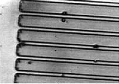
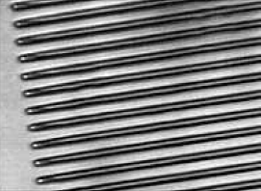
Once an oxidized wafer was spin-coated with photoresist, exposed to UV light, and patterned as outlined in section 4.2.2, the resulting photoresist pattern was investigated using an optical microscope. Fig. 5.5 shows optical images of two regions of oxide patterns. The most difficult photoresist pattern to obtain with the available equipment is the 2/2 $\mu$m region (cf. Fig. 4.2a) shown in Fig. 5.5b. In both cases, the photoresist is shown to be fully depleted between photoresist strips. Thus, the underlying oxide is fully exposed when etched with either etch method (section 4.2.3).
Figure 5-5. Optical Micrographs of Photoresist. a) Photoresist pattern from 2/5 $\mu\textrm{m}$ mask pattern. b) Photoresist pattern from 2/2 $\mu\textrm{m}$ mask pattern. |
The photoresist quality of oxide-patterned wafers is optically determined before proceeding with an etch procedure. Once the oxidized samples are etched, SEM images of the resulting oxide structures (Fig. 5.6) are acquired after the removal of photoresist. These oxide patterns are etched by the BOE method. The space between the oxide patterns has been fully etched away by BOE. However, there may still be residual oxide in the seeding channels that could be further removed by UV/ozone cleaning (section 4.2.4).
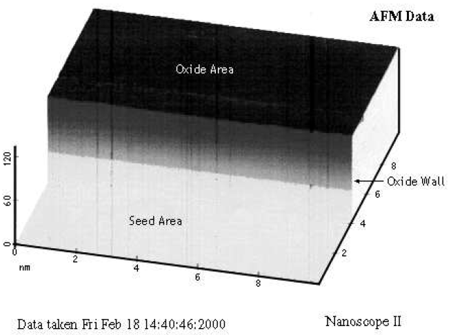
In one instance, after the use of RIE for oxide etching, an atomic force microscope (AFM) investigation indicates a sharp vertical interface (Fig. 5.7). The surface of the oxide and seeding areas both appear to be very smooth.
|
Figure 5.7. AFM of Vertical Oxide Wall and Seed Area. An AFM investigation of an oxide wall (formed by RIE) indicates that the vertical wall is sharply perpendicular to the base. The seed and oxide areas also appear smooth. |