In an earlier SMM-SOI Si(100) sample with 1000 Å RIE-patterned oxide, a cross sectional TEM investigation is performed. A $\sim2300$ Å Al mediator deposition occurs at room temperature ($T_{\textrm{Al}}=1100^\circ$ C, $P_{\textrm{op}}=1\times10^{-8}$ Torr). RHEED was unavailable for this early deposition. A buried $\sim7200$ Å Si film is deposited at $T_{\textrm{Al}}=350^\circ$C (9.8 keV, 0.1 A) at an operating vacuum pressure of $4\times10^{-7}$ Torr.
|
|
|
|
Figure 5-12. Cross Sectional TEM of SMM-SOI Si(100). The XTEM over oxide appears to be defect-free compared to the underlying quality of the substrate. The oxide thickness is measured to be $\sim300$ Å. The deposited Si is $\sim300$ Å thick. The Al film is estimated to be $\sim2300$ Å thick. |
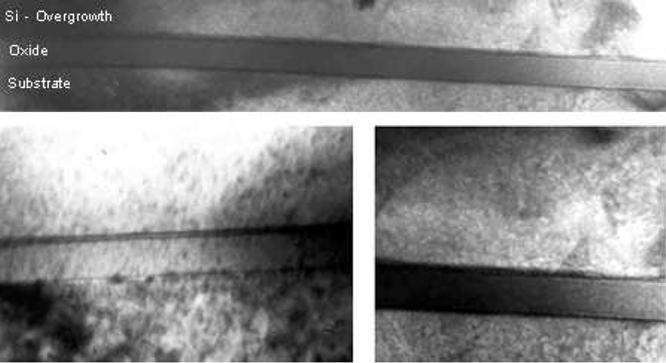
The cross sectional TEM images of this sample (Fig. 5.12) do not indicate any appreciable defects in the lateral overgrowth region. Unfortunately, no vertical oxide interfaces (oxide walls) were observed during XTEM investigations. In seeding areas, the deposited material appears to have been etched away during the TEM preparation stage, including Ar+ ion milling that prompted preventative measures such as the deposition of an a-Si cap layer on a few samples. Nonetheless, the identification of an oxide layer in the XTEM images (Fig. 5.12) is made. Small dark pits that appear in the TEM images are due to Ar+ ion milling. The quality of the lateral overgrowth of Si appears to be similar to the quality of the underlying Si substrate, assumed to be defect-free.
|
(a) (b) |
|
| Figure 5.13. Selected Area Diffraction (SAD) of SMM-SOI Si(100). a) SAD the entire region (both over and under the oxide layer) indicates p-Al, c-Al, and c-Si. b) SAD from over the oxide indicates the presence of c-Si, verifying single crystalline ELO of Si with SMM-SOI. |

Using the selected-area diffraction capabilities of the TEM, the electron beam is focused on the area of the cross sectional sample both over the entire region (substrate + oxide + overgrowth) with a large aperture and selectively above the oxide (only overgrowth material) with a smaller aperture. The resulting diffraction patterns (Fig. 5.13) indicate p-Al halos and c-Si diffraction spots with a slight presence of c-Al diffraction spots over oxide. Crystal lateral overgrowth of Si is verified for Si(100) SMM-SOI substrates. Given an unclean substrate of Si(100), SMM-SOI Si(111) is anticipated to yield equal or better overgrowth crystallinity.