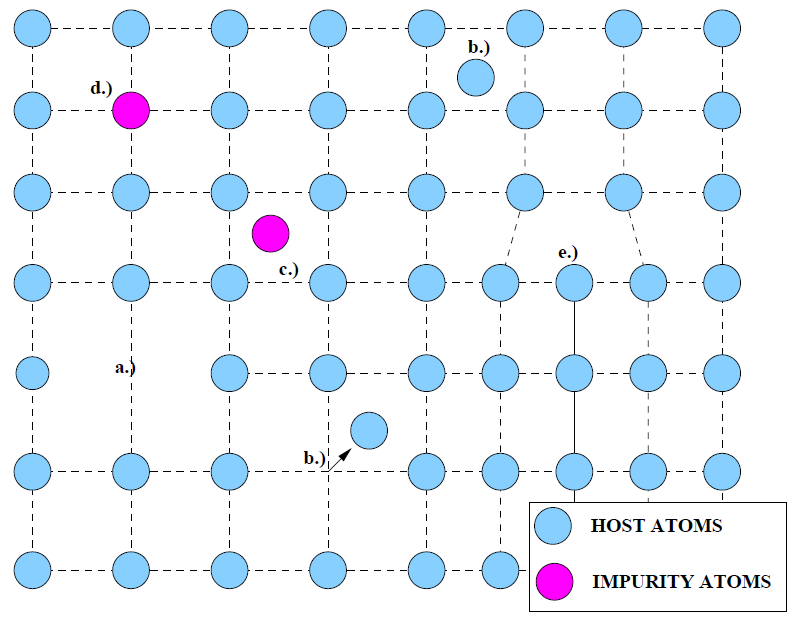
While there are numerous types of defects[1][2][3], a few are considered for illustrative purposes. The strain of an interface[4] induced during heteroepitaxy is the primary mechanism of dislocation formation in the grown thin film. A misfit dislocation is an entire line of atoms at the interface formed by an extra plane of atoms in the overlayer (Fig. 15b). Other defects that may be found in a crystal lattice are point defects, generally caused by displaced atoms or impurities. When an atom leaves a lattice site to occupy another site, the void created is called a vacancy, or Schottky, defect (Fig. 1.6a). Vacancies are present in even the most perfect crystals in thermal equilibrium since the entropy of the crystal is increased with an higher defect concentrations. If that atom remains at non-lattice sites between the planes of the crystal lattice, it is referred to as an interstitial, or Frenkel, defect (Fig. 1.6b).
An interstitial defect can also be formed by a foreign atom, or impurity (Fig. 1.6c). If the impurity atom fills in a vacant lattice site, it forms a substitutional defect (Fig. 1.6d). A high defect density can drastically reduce the electronic quality of a thin film. Several methods have been devised to minimize the density of defects. The method usually involves a period of annealing, or heating, after the deposition of the thin film. Annealing permits atoms to be thermally excited and vibrate until they fall into low energy lattice sites.
Defects in a host crystal thin film can inhibit or enhance the process of atomic diffusion[5]. When an impurity atom enters a vacant mediator lattice site (Fig. 1.6d) the process is considered substitutional diffusion. When a diffusor enters a site between the lattice planes of the host (Fig. 1.6c) it is considered interstitial diffusion.
Figure 1.6: Several Crystal Defects. a) Typical vacancy (Schottky) defect. b) Interstitial defect. c) Impurity interstitial defect. d) Substitutional impurity defect. e) Edge dislocation (cf. Fig. 1.5b). |
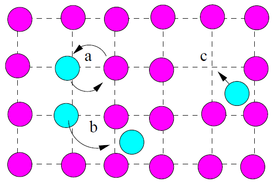
Vacancies can enhance the process of diffusion in several ways. A pair of atoms may interchange positions (Fig. 1.7a). The diffusor may migrate through a network of interstitial sites (Fig. 1.7b), or atoms may exchange positions with vacant lattice sites (Fig. 1.7c) These can all enhance or stunt the net diffusion of diffusors in the mediator[15].
Figure 1.7: Basic Diffusion Mechanisms. a) Shared rotation of two atoms, b) travel through interstitial sitesc and c) atoms fall into lattice vacancies. |
During the growth of a crystal thin film on a substrate, defects on the surface of the substrate are very easily replicated throughout the entire film structure. Lattice mismatches at the film/substrate interface may generate dislocations (Fig. 1.5b). It is imperative that necessary surface preparations be made to minimize the number of defects on a substrate surface and to minimize the interfacial strain between two mismatched lattices. The primary concern in the current investigation is with surface contaminants that may propagate unwanted defects in the overlayer. Substrate cleanliness will be discussed later.
References
- , “Misfit disclocations in lattice-mismatched epitaxial films”, Critical Reviews in Solid State and Materials Science, vol. 17, no. 6, pp. 507-546, 1992.
- , VLSI Technology. Bell Telephone Laboratory, Inc., 1983.
- , “Misfit dislocation generation in epitaxial layers”, Critical Reviews in Solid State and Materials Science, vol. 17, no. 3, pp. 187-209, 1991.
- , “Topics in Solid Phase Epitaxy: Strain, Structure and Geometry”, Materials Science and Engineering, vol. R16, no. 1, 1996.
- , “Diffusion and Defect Data - Solid State Data”. Trans Tech Publications, 1986.