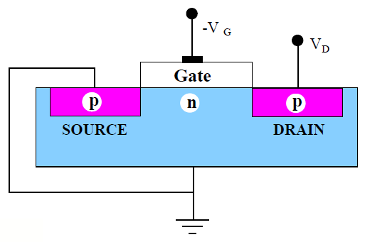
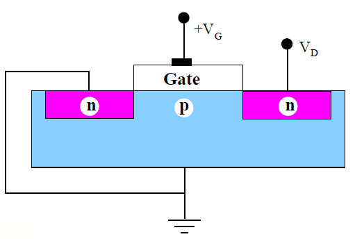
At the root of semiconductor device technology is the field effect transistor (FET). The metal-oxide-semiconductor field effect transistor (MOSFET)[1][2][3] is described for simplicity. The MOSFET consists of a source, gate, and drain shown schematically in Figure 1.1. Operation of a MOSFET involves grounding the substrate and source. For a p-channel MOSFET (PMOS) a small negative voltage is applied to the drain. An applied gate voltage controls the flow of current between source and drain (Fig. 1.1a). The source and drain may be heavily doped with positive p-type charges, or acceptors, (e.g. Al, B. Ga, and In atoms). The region immediately beneath the gate oxide is a region heavily doped with negative n-type charges, or donors (e.g. N, As, P, and Sb atoms). The gate oxide is commonly a silicon oxide (e.g. SiO2). When a large negative voltage is applied to the gate, the electrons in the n-type substrate are repelled away from the gate, leaving behind a positively charged p-type channel. For this reason, this space is called an inversion region that allows positive charges to flow from source to drain, thus completing the circuit and allowing current to flow through the transistor. The transistor is in its on state (e.g. a "1"-value) when a negative voltage is applied to the gate oxide. When a positive or zero voltage is applied, the transistor is in its off state (e.g. a "0"-value). This type of MOSFET is a p-channel MOSFET (PMOS) due to the nature of an inverted channel under an applied gate voltage. Likewise, a p-channel MOSFET (PMOS) may be fabricated and operated with a large positive gate voltage in the same manner described above. For the purpose of this thesis, references are made to the PMOS device due to the nature of materials investigated in SMME.
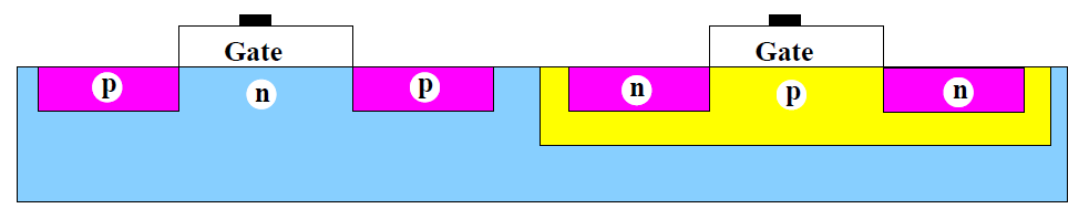
Figure 1.1: Metal Oxide Semiconductor Field Effect Transistors. a) PMOS has an n-type region beneath the gate. b) NMOS has a p-type region beneath the gate. c) A complementary MOS (CMOS) is a combination of a PMOS and NMOS fabricated, in this example, on an n-type substrate. |
||||
The ITRS outlines several parameter requirements for the semiconductor fabrication industry that should be met in order that the device technology would progress toward smaller features in a timely manner. Among the obstacles are thinner gates[4] of shorter length, shallow source and drain regions, and device isolation oxides[5]. A shortened gate length equates to a shorter on/off time (Fig. 1.2). That is, the transistor becomes faster. However, the principles of scaling require shallower dopant profiles, high doping concentration, and minimal thermal budget to avoid dopant diffusion[6][7]. In particular, the necessary strength of the negative applied gate voltage decreases as the channel depth decreases. On the other hand, silicon-on-insulator (SOI) can eliminate latch-up problems, decrease device processing steps, lower power consumption, and increase device speed. Before the advancement of silicon-on-insulator (SOI) device fabrication methods, transistors were typically isolated from each other by p-n junctions. In other words, an NMOS transistor would have an adjacent PMOS transistor.
As will be presented in subsequent chapters, SMME provides a unique solution to the aforementioned obstacles, among others, in a very low temperature process.
References
- , The Science and Engineering of Microelectronic Fabrication. Oxford University Press, 1996.
- , VLSI Technology. Bell Telephone Laboratory, Inc., 1983.
- , Solid State Electronic Devices. Prentice Hall, 1997.
- , “Effect of Buried Oxide Thickness in a Thin-Film Silicon on Insulator Power Metal-Oxide-Semiconductor Field-Effect Transistor”, Japanese Journal of Applied Physics, vol. 36, 1997.
- , “Generalized Guide for MOSFET Miniaturization”, IEEE Electron Device Letters, vol. EDL-1, 1980.
- , MOS Physics and Technology. Wiley, 1982.
- , Silicon Processing for the VLSI Era: The Submicron MOSFET, Vol 3. Lattice Press, 1994.