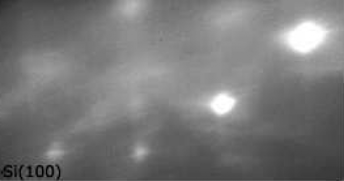
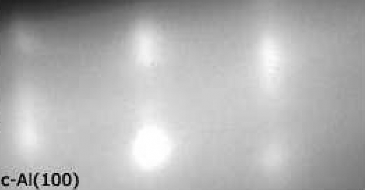
A blank Si(100) wafer is cleaned1 by heating to 750°C. The final-cleaned Si(100) surface remained unreconstructed (Fig. 5.3a), and is therefore not atomically clean. This may have led to the strong polycrystalline RHEED pattern (Fig. 5.3b) that records the progression of Al from a polycrystalline state into crystalline Al(100) (cf. Fig. C.1) during room temperature deposition, $\sim1$ hr ($P_{\textrm{op}}=1\times 10^{-8}$ Torr). This orientation of Al is not in agreement with[1] where Al(110) was shown to grow on reconstructed Si(100)$2\times 1$. However, since the surface was not shown to be reconstructed after final cleaning (Fig. 5.3a), the grown Al was not properly oriented with the formation of Al-dimers,[1] and thus resulted in Al(100) growth on Si(100).
Figure 5.3. RHEED Investigation of SMME Si(100). a) Partially cleaned Si(100) surface (no $2\times 1$ reconstruction). This demonstrates Si crystallinity with considerable contamination. b) Development of Al mediator deposition initially shows p-Al (faint rings) that later transforms into c-Al(100) c.) RHEED after Al mediator deposition. d) The disappearance of diffraction spots indicates that the electron beam is incident on an area of the wafer with Si deposition. e.) c-Al(100) remains after deposition of Si diffusors at $350^\circ\textrm{C}$. The center beam direction is indicated by "$\times$". |
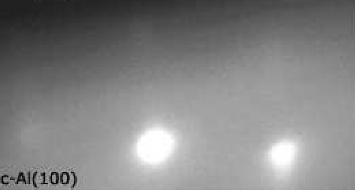
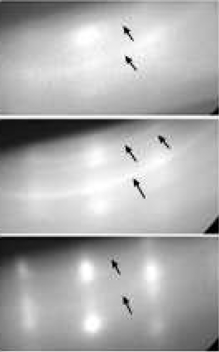
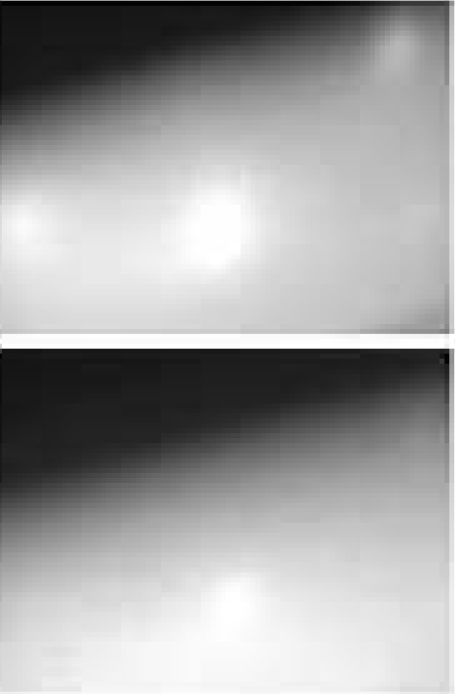
The substrate is then heated ($\sim15^\circ$C/min) to $350^\circ$C at which time Si is deposited from the electron beam evaporator (9.8KeV, 0.1A) for 70 min. The disappearance of diffraction spots during initial stages of Si deposition (Fig. 5.3d) verifies the electron beam location on the Si-deposition area. After SMME Si deposition, RHEED indicates strong c-Al(100) (Fig. 5.3e) on the surface indicating that Si atoms have diffused into the Al mediator layer.
|
Figure 5.4. SEM Micrographs of SMME Si(100). a) Substrate with only Al mediator coverage. b) Region of SMME region containing a buried Si layer, Al film, and capped with an a-Si layer. The surface appears somewhat more rough than in (a), however, this is largely due to the presence of an amorphous Si cap layer. |
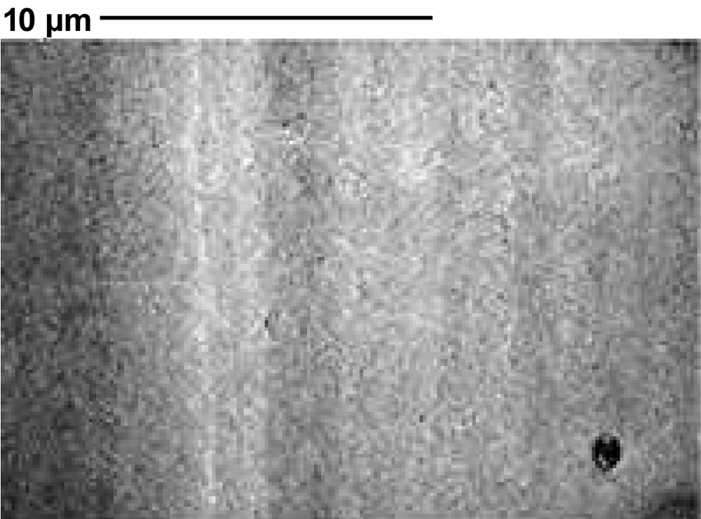

The initial Al mediator film (Fig. 5.4a) is shown by SEM to be smooth. The resulting SMME-deposited region is shown to be somewhat rougher (Fig. 5.4b).
References
- , “Solid-Metal Mediated Molecular Beam Epitaxy (SMM-MBE) of Si(111) at a Buried Inteface: A New Epitaxial Growth Method”, in 42nd National AVS Symposium, Minneapolis, MN, 1995.
- 1. In this case, the heater was unable to acquire a higher temperature as current to the heater was fully saturated.