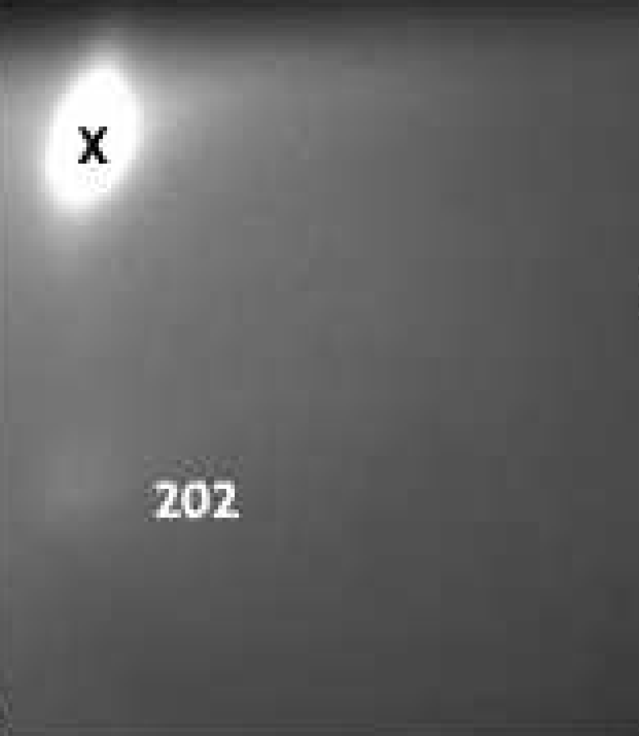
A blank Si(111) wafer is placed in the UHV MBE system with a base pressure of $\sim1\times10^{-9} \textrm{Torr}$. The wafer is initially cleaned by substrate heating to 830°C followed by deposition of a Si buffer layer at substrate temperature, $T_{\textrm{s}}=750^\circ\textrm{C}$, (buffer thickness, $\theta_{\textrm{buffer}}\approx 600 $Å). The Si buffer layer is used to provide a new, atomically clean surface prior to the experiment. A clear $7\times 7$ diffraction pattern is typically obtained after thermal cleaning. Following cleaning, an Al mediator layer is deposited from an effusion cell source ($T_{\textrm{Al}}=1175^\circ\textrm{C}$) at room temperature for 20 minutes.
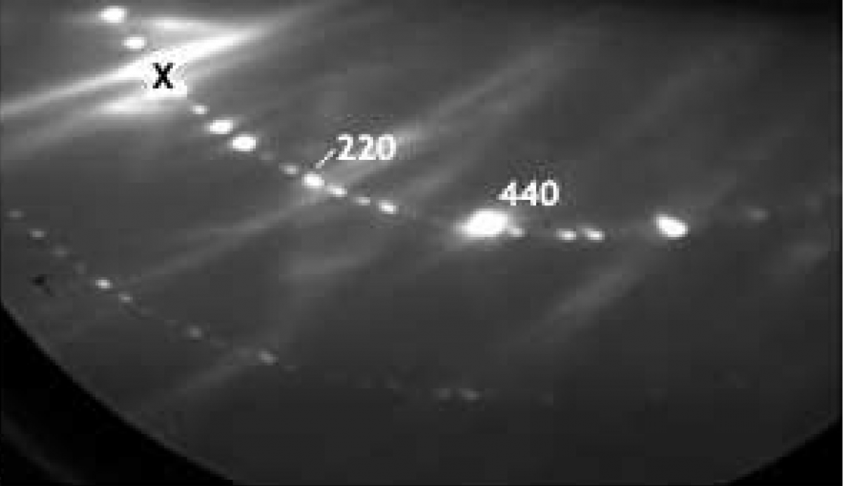
Once the deposition of an Al mediator begins, RHEED indicates the temporary existence of p/c-Al (Fig. 5.1b). A c-Al(111) mediator is observed (Fig. 5.1c) after Al deposition (cf. Fig. C.3). Next, the substrate is heated to $250^\circ\textrm{C}$ at $10^\circ\textrm{C}/\textrm{min}$, then to $350^\circ\textrm{C}$ at $14.5^\circ\textrm{C}/\textrm{min}$. Si was then deposited from an electron beam evaporator (9.5 keV high voltage, 0.1 A emission current) while keeping the sample at $T_{\textrm{s}}=350^\circ\textrm{C}$. After 7.5 minutes of Si deposition, another RHEED pattern is recorded to verify that the electron beam is incident at a location of Si deposition (absence of diffraction spots in Fig. 5.1d, cf. Fig. 5.1c). Once the substrate is cooled to room temperature, the initial c-Al(111) (Fig. 5.1c) recorded before Si deposition remains (Fig. 5.1e).
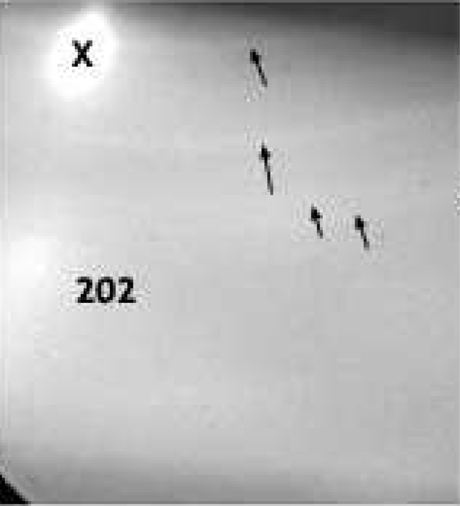
Figure 5.1. RHEED Investigation of SMME Si(111). a) $7\times 7$ surface reconstruction indicating clean Si(111) surface after 600 Å Si buffer layer. b) Measured during initial stages of Al mediator deposition. The appearance of faint rings (arrows) indicate p-Al with c-Al(111), c) c-Al(111) after deposition (cf. Fig. C.3), d) disappearance of c-Al diffraction spots 5 minutes into Si deposition verify that the Si diffusors are being deposited at the RHEED beam spot location, and e) c-Al(111) remains after deposition of Si at $T_{\textrm{s}}=360^\circ\textrm{C}$. Note: The "$\times$" indicates the center diffraction spot. The sample holder geometry does not permit on-axis diffraction. The sample was slightly rotated off-axis to show the full diffraction features. |
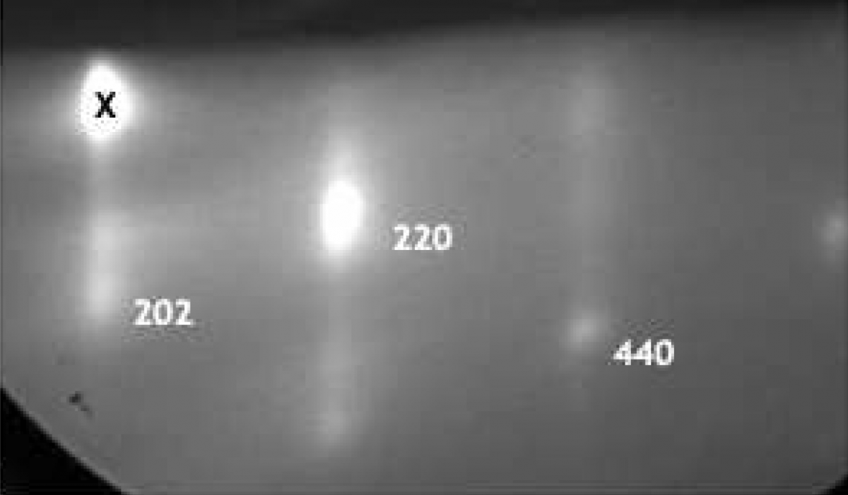
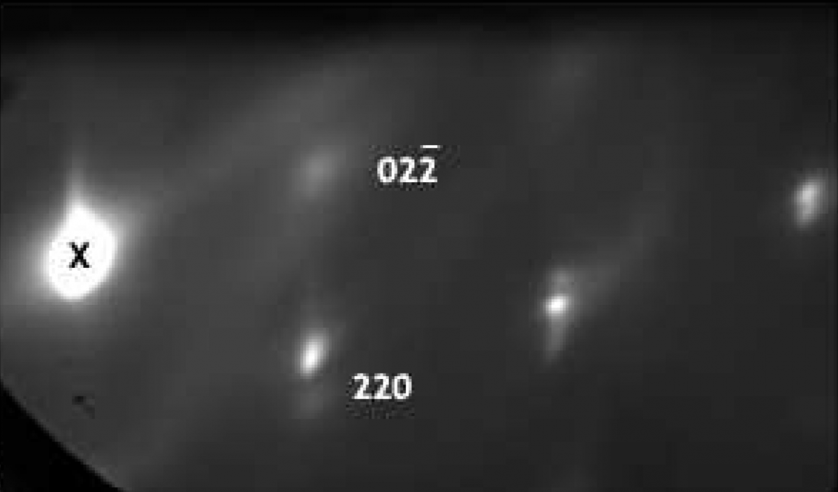
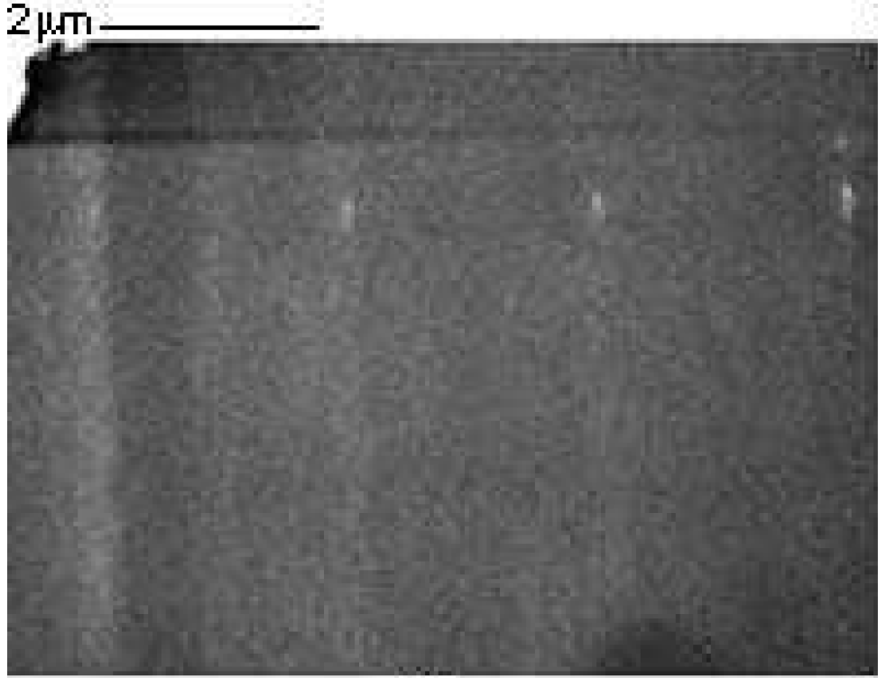
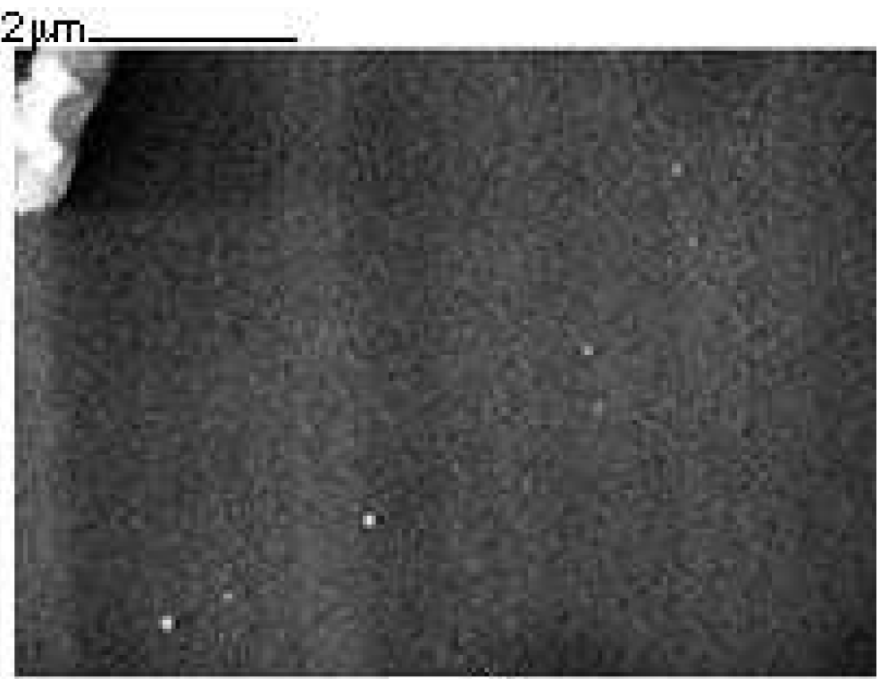
RHEED analysis shows that Si atoms have diffused into the Al mediator. The Al mediator remains crystalline after the entire SMME process despite the temporary appearance of p-Al (Fig. 5.1b). The Al mediator film is initially smooth when deposited (Fig. 5.2a). This is anticipated by the vertical spikes in the RHEED pattern (Fig. 5.1c). After deposition, Si has diffused into the Al mediator, leaving behind a smooth Al surface (Fig. 5.2b), but slightly rougher than before Si deposition, as anticipated by the crystallinity measured by RHEED (Fig. 5.1e). An amorphous Si cap layer1 is deposited for 5 minutes ($\sim400 $Å).
SMME on Si(111) has been previously investigated.[1] Al(111) was shown to grow epitaxially at room temperature. In these investigations, Al(111) was also shown by RHEED to remain on the surface after Si diffusor deposition at $400^\circ\textrm{C}$.
|
Figure 5.2. SEM Micrographs of SMME Si(111). a) Substrate area with only Al mediator coverage. b) Substrate region of SMME region (Al mediator covering Si diffusor layer with an amorphous Si cap layer). Both regions are relatively smooth, indicating minimal damage done to the Al mediator, and no Al island formation. |
References
- , “Epitaxial Growth of Si(111) at Buried Interfaces Using Solid-Metal Mediated Molecular Beam Epitaxy”, in 1996 MRS Spring Meeting, San Francisco, CA, 1996.
- 1. An amorphous cap layer is deposited on several samples in an attempt to prevent ion milling of Al layers during the final stages of TEM sample preparation.