Oxide is removed from the exposed regions of the wafer (Fig. 4.1d) using an oxide etch (Fig. 4.1e). Two methods of oxide etch are used: buffered oxide etch (BOE) and reactive ion etch (RIE). BOE is an isotropic wet etch process that includes a solution of hydroflouric acid (HF) and ammonium flouride (NH4F) used to avoid unwanted removal of photoresist. The etch rate of oxide is 800 Å/s at $23^\circ\textrm{C}$. The isotropy of BOE causes tapering of the oxide walls (Fig. 4.3a).
|
(a) (b) Figure 4.3. Buffered Oxide and Reactive Ion Etch (RIE). a) BOE is an isotropic etching process that causes tapering of the etched material. b) RIE is an anisotropic etching process that produces a sharp vertical interface of the etched material. (cf. Fig. 5.7) |

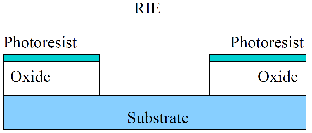
In RIE, an etching gas (e.g. CCl2F2) is charged to generate a plasma (Fig. B.3). Charged particles in the plasma are accelerated across the grounded substrate and selectively etch oxide regions faster than the photoresist. RIE is an anisotropic etch method that provides a sharp vertical edge of the etched material (Fig. 4.3b).
While the anisotropy of RIE is desired for SMM-SOI, it also tends to damage the underlying substrate surface. BOE has been used with considerable success. Though both methods have been used, a controlled comparison of these two methods was not made during this investigation.