The oxidized wafer surfaces are patterned by a photolithographic procedure as follows. The wafer is spin-coated with photoresist (Fig. 4.1b) at 4000 RPM for 60 s, then soft baked on a hot plate at $115^\circ \textrm{C}$ for an additional 60 s. Next, the wafer is aligned with a chrome mask1 that provides the necessary patterns of oxide dimensions investigated (Fig. 4-2a). A variety of oxide/seed dimensional ratios are used to investigate the dimensional relationship, $s/w$, of SMM-SOI (Fig. 4-2b).
|
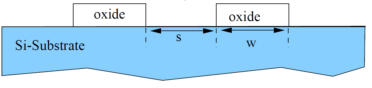
(a) (b) Figure 4.2. Photolithographic Mask & Seed/Oxide Dimensional Ratio. a) Schematic of chrome mask used for patterning oxide. Ratios indicate seed/oxide ($s/w$) lateral dimensions (microns) of respective pattern regions. b) A cross sectional perspective of the seed/oxide dimensional ratio. |

The chrome mask is gently placed over the photoresist-covered wafer (Fig. 4.1c). The areas of the wafer not covered by the chrome pattern are exposed to a 150 W UV lamp for 10 s. Once the mask is carefully removed, the wafer is developed in a 1:1 solution of deionized water:developer for 60 s. The developed photoresist (Fig. 4.1d) is then hard baked at $90^\circ\textrm{C}$ for 20 minutes.
- 1. Chrome mask, designed by F. B. Sharer and M.-A. Hasan, was fabricated by an outside company.