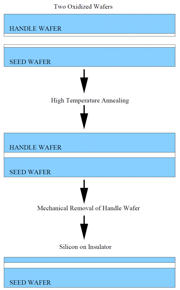
The generic wafer bonding process (Fig. 3.4a) makes use of two wafers. Surfaces of a heavily doped seed wafer and a lightly doped handle wafer are thermally oxidized. The two oxidized wafers are then pressed together, oxide to oxide, and placed in an oxidizing environment at temperatures greater than $700^\circ \textrm{C}$ to seal the oxidized faces (Fig. 3.4a). The handle wafer is then mechanically polished to the required device depth. The surface of the resulting device layer is polished to device-quality, and the remaining substrate is the required SOI structure (Fig. 3.4a). The oxide thickness can range from native oxide to 1000 Å.
Figure 3.4. Wafer Bonding Methods. a) Wafer bonding begins with the thermal oxidation of two silicon wafers. The wafers are brought together and annealed to bond the two oxide faces. The handle wafer is mechanically polished to the required device-layer thickness. b) A greatly improved wafer bonding technology, SmartCut®, makes repeated use of the handle wafer. The handle wafer is first implanted with a buried film of hydrogen atoms. The wafers are bonded, oxide-to-oxide, and thermally annealed. The handle wafer is stripped away at the hydrogen-rich film depth, polished and reused for several such processes. |
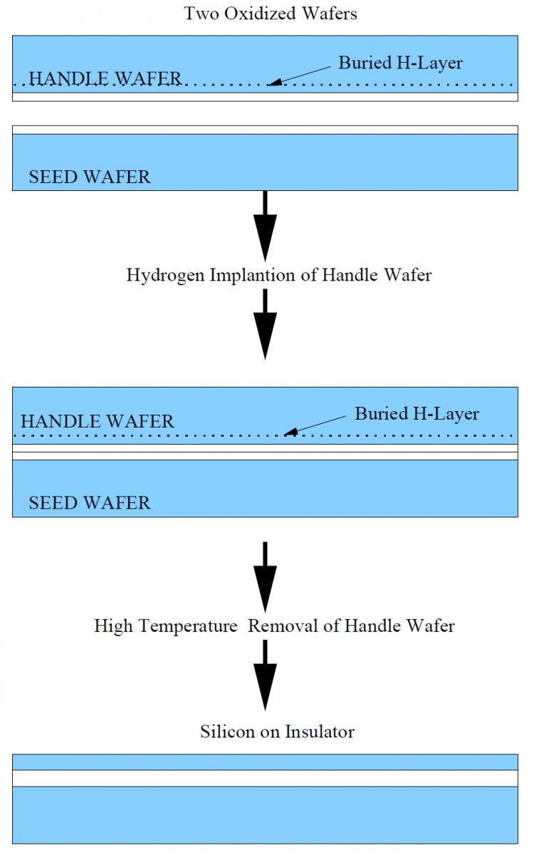
The basic wafer bonding process sacrifices an entire wafer for every SOI wafer manufactured. A more efficient method has been devised, the SmartCut® process[1][2] (Fig. 3.4b), that permits repeated use of the same handle wafer. In the SmartCut® process, both wafers are similarly oxidized as before, but the handle wafer is implanted with a layer of low-energy hydrogen. The energy of the implanted hydrogen ions determines the depth at which the hydrogen-rich layer will form. The diffusing hydrogen atoms are much too small to affect the crystallinity of the silicon. The two wafers are then bonded together as before. The shallow buried hydrogen layer provides a perforation-like interface that allows the handle wafer to be easily removed during a final thermal cycle of the bonded wafers. The remaining handle wafer is then polished and reused.
Wafer bonding methods, though effective, require several mechanical processing and heating cycles. SMM-SOI requires no mechanical steps nor high temperature annealing cycles, making it a more efficient fabrication technology.
References
- , “Basic mechanisms involved in the Smart-Cut® Process”, Microelectronics Engineering, vol. 36, no. 1-4, pp. 233-240, 1997.
- , “The History, Physics and Applications of the Smart-Cut® Process”, MRS Bulletin, vol. 23, no. 12, pp. 35-39, 1998.