With the development of several parameters and considerations in the previous chapter, the technology of SMME can be considered for use as a viable silicon-on-insulator (SOI) fabrication technology.[1] The extension of SMME to a solid-metal-mediated silicon-on-insulator (SMM-SOI) technology comes as a result of observations made (Fig. 3.5) during the original experiments[2]. A perfectly grown Si thin film at a buried Si/Al interface would be ideally indistinguishable from the Si(111) substrate by cross sectional transmission electron microscopy (XTEM). The investigators had allowed a partial monolayer of Al, deposited on the substrate, to oxidize. The resulting Al oxide islands were used as markers of the original substrate interface.
|
Figure 3.5. SMME Cross-Sectional TEM. The nanoclusters of Al oxide used to mark the original substrate/mediator interface appear transparent to the SMME process. There are no noticeable defects over these islands. ([2], used with permission.) |
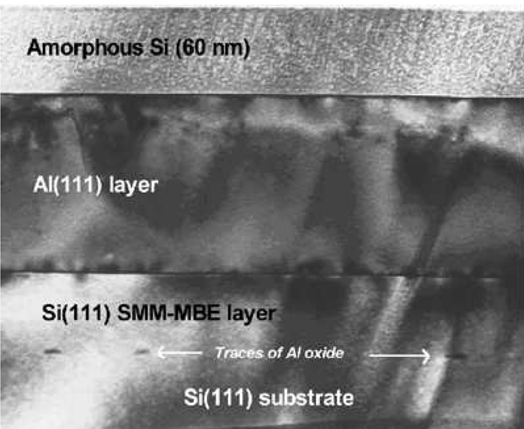
Two important observations can be made from Fig. 3.5. First, the small oxide islands ($\sim10 \textrm{nm}$) do not appear to cause defects in the growth of the buried SMM-Si thin film. This indicates that the affect of buried Si/Al interfacial growth of Si permits uniform epitaxial lateral overgrowth (ELO) of the Si thin film over the oxide. The vertical Al/Al2O3 interface is abrupt and has been shown to vary by no more than two atomic spacings.[3] Thus, the oxide base should not produce an environment in which facets can flourish as in the SPE environment (Fig. 3.2). Instead, c-Al should grow uninterruptedly up the oxide wall. Additionally, if SMME growth is characterized by the proposed Al-Al dimer kick-out mechanism (section 2.5.1) it may be very unlikely for dangling Si diffusor bonds to remain dangling (thus the two-undistorted bond requirement is enforced in strength) that further minimizes the potential for facet formation near the oxide walls.
Another important observation from Fig. 3.5 is that the Si diffusors have not diffused through the Al oxide islands. Otherwise, the islands would have been moved along with the Al mediator film. The process of SMME appears to be essentially transparent to the presence of oxide islands.
For the current investigation, Si substrates are oxidized in a nitrogen ambient thermal oxidation furnace. The oxide thickness, $\theta_{\textrm{ox}$, ranges from 250 Å to 1000 Å. The oxide film is etched to provide larger oxide islands ranging from $2 \mu\textrm{m}$ to $500 \mu\textrm{m}$ in width.
An aluminum mediator is then deposited uniformly to form regions of single- and double-domain Al in seeding areas. Along the vertical and horizontal oxide/Al interfaces, nanocrystalline grains of Al2O3 coat the oxide region. As previously mentioned, the vertical interfaces are considerably abrupt and vary by no more than a few lattice spacings. In regions over oxide, the Al mediator film is anticipated to be crystalline as a result of lateral overgrowth using the crystalline seed. However, polycrystalline Al may also exist. The resulting mediator structure has regions of uniform crystallinity (over seed areas) and regions of crystalline/polycrystalline Al (over oxide areas).
|
(a)
(b)
(c) Figure 3.6. Basic SMM-SOI Process. a) Oxide islands are formed and covered by an Al mediator film. Si diffusor deposition begins. b) Si begins to form an SMME growth front in the seeding areas (between oxide islands). Once the SMME growth front has reached the height of the oxide islands, epitaxial lateral overgrowth (ELO) begins until the oxide is covered c) forming a buried crystalline diffusor layer on oxide. The mediator film is available for subsequent SMM-SOI fabrication stages. |
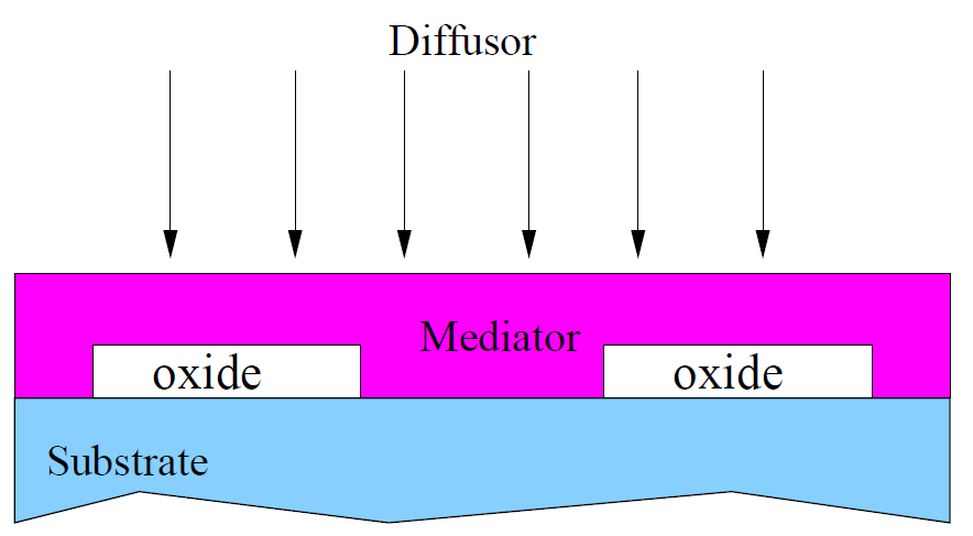
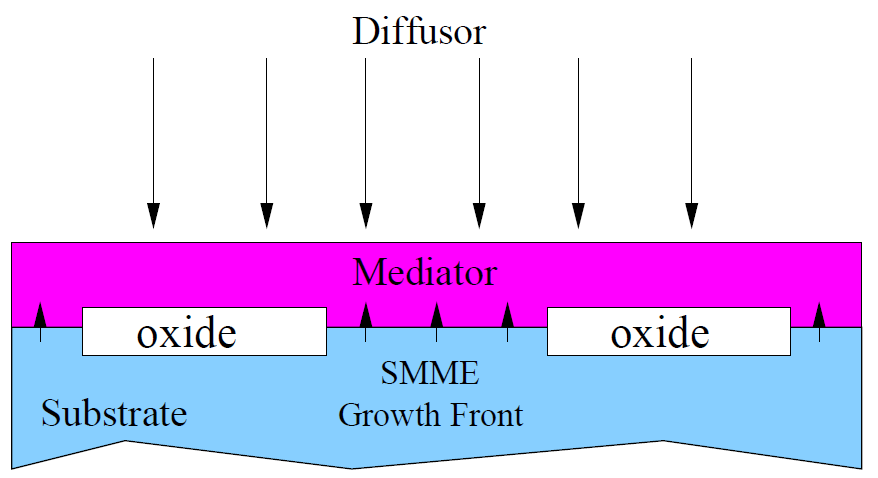
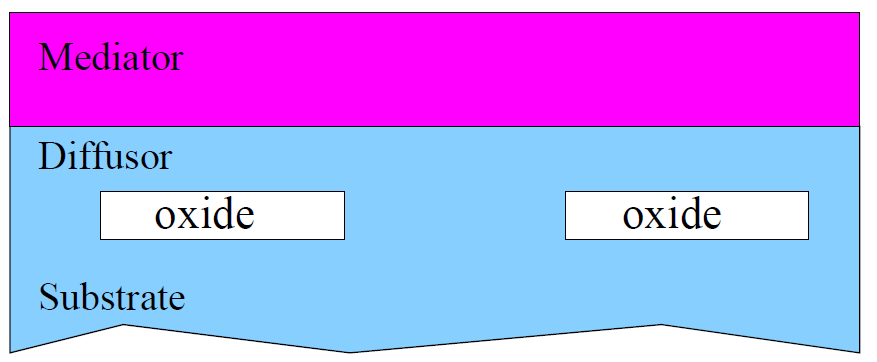
Next, a Si diffusor is deposited (Fig. 3.6a) at a low substrate temperature. At first, an interim monolayer of Si atoms is present at the Al mediator surface. Once the surface diffusor concentration is large enough, the Si begins to rapidly diffuse into the Al mediator. The shower of diffusors is uniform across all regions of the sample (oxide and seed regions). Since the rate of deposition at the Al surface can be controlled, it provides a constant flux of diffusors into the Al mediator. However, there is a distinct difference between oxide and seed regions. The seed region readily passes the diffusors to the buried Si/c-Al interface. Once the diffusors are incorporated at this buried interface, they no longer contribute to the bulk mediator concentration of diffusors. Instead, the buried film grows and pushes the Al mediator film away from the substrate as an SMME growth front (Fig. 3.6b). The ideal resulting structure (Fig. 3.6c) includes c-Si regions over oxide.
References
- , “Fabrication of Buried Oxide Structures at Low-Temperature ($T_s\lt 500^\circ$C) Using Solid-Metal-Mediated Molecular Beam Epitaxy”, in AVS - First International Conference on Microelectronics and Interfaces, Santa Clara, CA, 2000.
- , “Solid-Metal Mediated Molecular Beam Epitaxy (SMM-MBE) of Si(111) at a Buried Inteface: A New Epitaxial Growth Method”, in 42nd National AVS Symposium, Minneapolis, MN, 1995.
- , “Structure of the Al/Al2O3 interface”, Appl. Phys. Lett., vol. 46, 1985.