Once the Si atoms have completely diffused through the Al layer they are incorporated into the low-energy lattice sites of the c-Si (Fig. 2.4c) interface and no longer contribute to the net diffusor concentration in the mediator bulk.
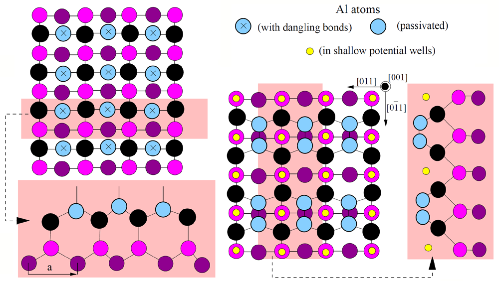
The c-Al/c-Si(100) interface has been previously investigated[1]. The Si(100) surface is typically cleaned by inducing a $2\times 1$ surface reconstruction by heating (Fig. 1.14). The first monolayer of Al atoms deposited on the reconstructed Si(100) $2\times 1$ surface has been shown[1] to break the Si-Si dimer bonds and subsequently passivate their own bonds by forming very strong Al-Al dimers (Fig. 2.6c). The second monolayer of Al atoms has been shown to fill potential wells in the middle of two Al dimers followed by occupancy of shallow potential well sites between dimer pairs. The required Al bond length along the $\langle110\rangle$ direction is approximately equal to the natural bond length of the Al lattice along this direction. It has been argued that the growth of these two monolayers forms the template for additional Al(110) layers. Thus, c-Al(110) is grown on the Si(100) $2\times 1$ surface at room temperature.
|
Figure 2.6. Al Addimer Formation on Si(100) $2 × 1$ Surface. a) The first monolayer of Al atoms breaks the Si-Si dimer bonds of the original $2 \times 1$ reconstructed Si(100) surface. This leaves dangling Al bonds. b) Cross sectional perspective of (a). c) The dangling Al bonds are passivated by attaching to neighboring Al bonds, thus forming Al addimers perpendicular to the direction of the original Si dimers. d) Cross sectional perspective of (c). The second monolayer of Al atoms begins to take up location in shallow potential wells between Al-dimers along the [011] direction (c) & (d). |
The Al/Si interface is mostly free of misfit dislocations typical of other heteroepitaxially grown structures. Instead, due to the thermal mobility afforded by the shallow potential wells along the Si(110) direction, it has been shown that a larger cell of Al planes can be better-matched to a cell of Si planes in such a way as to drastically reduce the otherwise large strain at the Al/Si interface. In particular, it has been suggested that four Al(110) planes can be matched to three Si(110) planes with only 0.7\% mismatch, and 21 Al(001) planes match to 20 Si(011) with only 0.45\% mismatch. These percentages are very small compared to 1:1 planar matching that results in 25.5\% and 5.5\% mismatches for respective directions. The number of dislocations is statistically minimized in the resulting c-Al(110) film.
The dimerized Al-Al bonds at the buried interface are much stronger than Si-Al bonds (Fig. 2.6d). The diffused Si atoms are most likely to break respective Si-Al bonds and form Si-Si bonds that simply serve to continue the underlying bulk Si(100) lattice structure. Subsequent diffusor layers progress in the template of the Si(100) crystalline structure. An Al-Al dimer "kick-out'" mechanism is proposed to dominate the incorporation of Si diffusors at the buried c-Al(110)/c-Si(100) interface. Growth on the Si(111) $7\times 7$ reconstructed surface is anticipated to progress in a similar manner as to replicate the underlying bulk Si crystal lattice structure as has been shown by the original SMME experiments for Si(111)[2].
References
- , “Epitaxial growth of Al on Si by thermal evaporation in ultra-high vacuum: growth on Si(100)2x1 single and double domain surfaces at room temperature”, Surface Science, vol. 236, 1990.
- , “Solid-Metal Mediated Molecular Beam Epitaxy (SMM-MBE) of Si(111) at a Buried Inteface: A New Epitaxial Growth Method”, in 42nd National AVS Symposium, Minneapolis, MN, 1995.