Assumptions governing Si diffusion and incorporation have led to the proposed use of an atomistic model based on the Drosd-Washburn model[1] that has been used to explain defect formation in solid phase epitaxy (SPE) experiments. In the Drosd-Washburn model, the necessary requirement for crystal growth is the formation of two undistorted bonds by Si atoms present in an amorphous layer crystallized by thermal annealing. An undistorted bond is a complete bond between two Si atoms of the same Si-Si bond length as the underlying crystal.
Since there are no anticipated dislocation defects in the grown c-Al crystal, the question of a model turns to the growth characteristics of the SMM growth front (Fig. 2.3b). The growth of a buried SMM Si layer is anticipated to progress more rapidly on one substrate orientation than the other, as predicted by the proposed variation of the Drosd-Washburn model. The proposed model allows for breaking of Al-Si bonds at the Al-Al dimer sites (Fig. 2.6d) by the diffused Si atoms. The proposed growth model is characterized by an Al-Al dimer "kick-out" mechanism that relieves the strain of Al-Si bonds caused by strong Al-Al dimer bonds. As the Si atom attaches to two underlying Si-bonds, the two remaining Si bonds of the diffused atom may be passivated by the Al dimer itself. The second monolayer of buried Si diffusors work to break the newly formed Si-Al bonds, strained by the Al-Al dimer pairs and likewise, repeatedly progress layer by layer. The SMM growth front proceeds in a manner similar to the arguments made by the Drosd-Washburn model that is in agreement with an earlier model that enforces a condition of surface stability by the completion of hexagonal bond structures. The Drosd-Washburn model is such that the number of undistorted bonds completes the stable hexagonal structure requirement.
|
Figure 2.7. Drosd-Washburn Atomistic Growth Direction Model. The Si(100) direction requires one atom per grown layer to complete the stable two-undistorted bond requirements (corresponding to the completion of a hexagonal structure). Si(110) requires 2 such atoms, and Si(111) requires 3. Statistically, the potential for creating a new stable layer is greatest in the Si(100) direction and smallest in the Si(111) direction. |
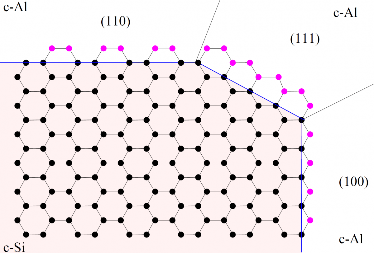
Statistically, the Si(100) direction requires one Si atom to complete the next stable monolayer of diffusor atoms. The Si(110) requires two atoms. The Si(111) direction requires three atoms (Fig. 2.7). This difference statistically implies that the Si(111) direction has a slower growth rate than Si(100) and Si(110) directions. Experimentally, the Si(110) direction of growth is at least an order of magnitude slower than the Si(100) growth direction. The growth rate along Si(100), $v(100)$, is much faster than along Si(111), (i.e. $v(100) \gg v(111)$).[2] The key to growth rate is the ability to form a stable layer of undistortedly bonded diffusors. The Si(100) direction forms a stable layer more rapidly than Si(111) (Fig. 2.8).
|
Figure 2.8. Drosd-Washburn Atomistic Growth Model for Si(100). At an a-Si/c-Si interface, during annealing, a-Si atoms must form two undistorted bonds (a) with the c-Si surface in order to form a stable monolayer of atoms. The requirement of completing the stable hexagonal bonds (b) $\pi$-bonds} as described earlier, is essentially the same as enforcing the "two-undistorted bond" requirement. |

A uniform growth of buried Si thin film by SMME is best generated by a slow deposition such that diffused Si atoms have sufficient incorporation time at the buried interface. The deposition rates used in the original experiments were $\lt 2$Å/s. However, an upper limit of the SMM growth rate may be observed if the Si(111) buried interface, for example, becomes saturated with unincorporated diffusors that may distort crystal orientation. This may occur more readily in the Si(111) direction as the time required to successfully form a stable layer is dependent upon the proper statistical alignment of 3 atoms rather than the time required to form a stable layer with only 1 atom as in the Si(100) direction.
While the current investigation does not examine the respective directional growth rates directly, several observed phenomena are partially explainable as a consequence of these mechanisms when combined with another model related to the anticipated diffusor dynamics when SMME is proposed for use as a fabrication method for SOI structures. This is considered in the following chapter.
References
- , “Some observations on the amorphous to crystalline transformation in silicon”, J. Appl. Phys., vol. 53, 1982.
- , “Solid Phase Epitaxial Growth of Si Through Al Film”, Proceedings of the Symposium on Thin Film Phenomena Interfaces and Interactions, vol. 78. p. 293, 1978.