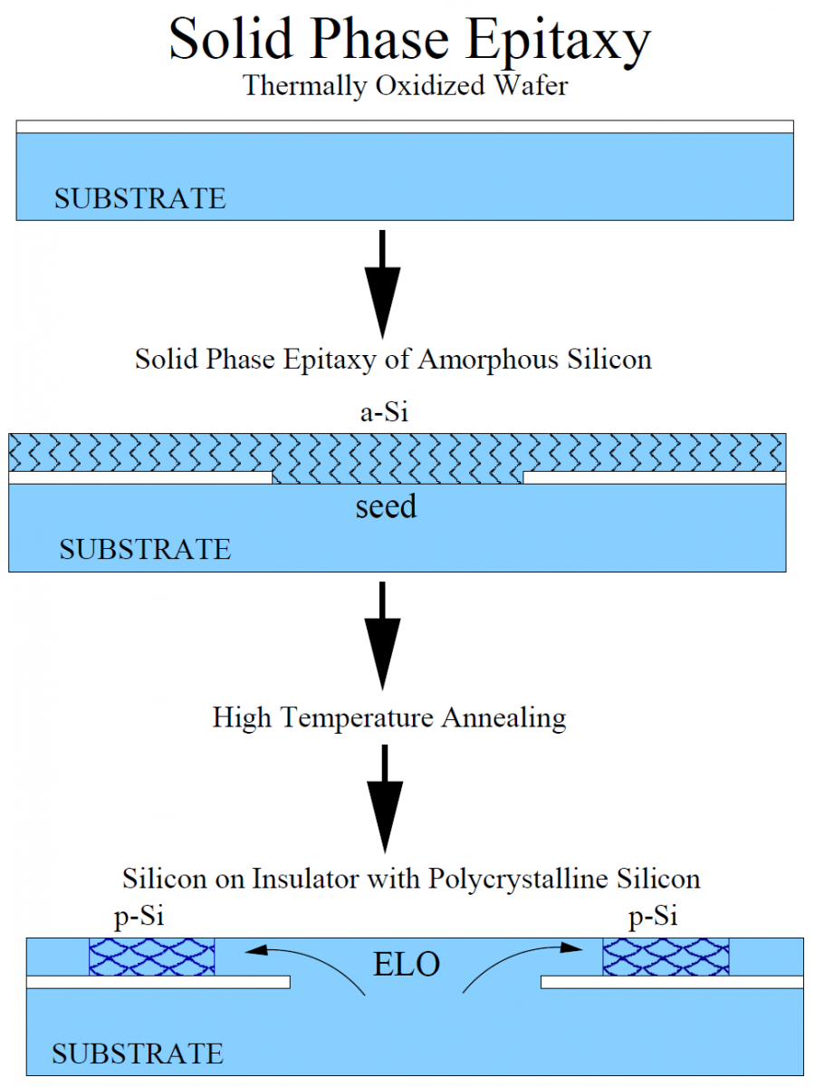
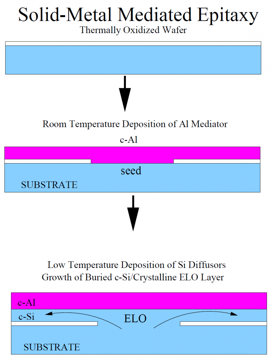
The solid phase epitaxial SOI fabrication method[1] (Fig. 3.1a) is similar to the SMM-SOI process[2] (Fig. 3.1b). The wafer is first thermally oxidized, patterned, and etched to generate seed areas in the oxide -- a process described later. An amorphous silicon (a-Si) film is deposited atop the entire structure then thermally annealed for several hours (sometimes days) to allow the a-Si film to crystallize.[3] The quality of the crystallized silicon device layer over oxide is typically very poor, and the extent of the lateral overgrowth is severely limited by the inevitable premature formation of polycrystalline silicon (p-Si) on the oxide that prevents long range lateral crystal silicon overgrowth. Despite some advances in recrystallizing the a-Si layer, lateral overgrowth of only a few microns of crystalline silicon have been reported. While this technology may be useful for the small-dimensional requirements of current and future ULSI technologies, the process requires several costly fabrication stages to avoid its many obstacles.
|
Figure 3.1. Solid Phase Epitaxy vs SMM-SOI. a) A wafer is thermally oxidized and patterned. An a-Si film is deposited across the entire sample then annealed at a high temperature. The a-Si crystallizes in seed areas as a result of annealing; p-Si forms in oxide regions due to the absence of an appropriate seed. b) SMM-SOI is similarly oxidized and patterned. However, a c-Al film is deposited at room temperature. Once heated to a low substrate temperature, Si is deposited on the Al film and diffuses to the buried Si/Al interface where it grows vertically upward in seed areas then laterally over oxide regions. |
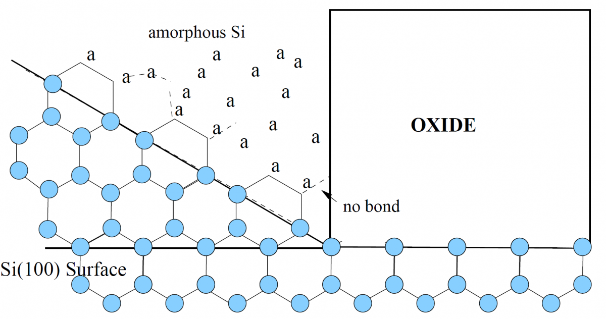
One obstacle encountered in SPE-SOI is the inevitable formation of facets along the oxide/substrate boundary (Fig. 3.2) explained in terms of the Drosd-Washburn model. A facet can easily form as a failure of the formation of two undistorted bonds of the a-Si atoms near the base of the oxide wall. Atoms in an a film atoms cannot form undistorted bonds with the oxide and an atom nearest the oxide base does not contribute to the formation of the first monolayer of c-Si. Subsequent atomic monolayers can only attach to the c-Si formed. Thus, a facet plane develops away from the oxide wall. Once this occurs there is no chance of seed formation for lateral overgrowth once the c-Si layer exceeds the height of the oxide wall. Despite localized facet formation, SPE-SOI remains successful in unaffected regions. A better understanding of the SPE-SOI process[4][5] has provided several advances of this fabrication method. Such pieces of technology may likewise help to improve the SMM-SOI fabrication method.
|
Figure 3.2. SPE-SOI Facet Formation. SPE SOI is plagued by facet formation near oxide walls where the two-undistorted bond requirement is not met. This unmet growth condition spawns into a facet plane away from the oxide wall. |
SMM-SOI is virtually transparent to several obstacles inherent to SPE-SOI. ELO of SMM-SOI has been demonstrated to provide hundreds of microns of crystalline lateral overgrowth. The longest lateral overgrowth observed in the current investigation is $250 \mu\textrm{m}$. As well, due the environment near the oxide base, SMME is shown to be nearly free from facet defect formation. This unique feature will be discussed later.
References
- , “Formation of a Silicon-On-Insulator Structure by Solid Phase Epitaxy”, in Silicon On Insulator: Its Technology and Applications, 1985.
- , “Fabrication of Buried Oxide Structures at Low-Temperature ($T_s\lt 500^\circ$C) Using Solid-Metal-Mediated Molecular Beam Epitaxy”, in AVS - First International Conference on Microelectronics and Interfaces, Santa Clara, CA, 2000.
- , “Lateral solid phase epitaxy of amorphous Si films onto nonplanar SiO2 patterns on Si substrates”, Appl. Phys. Lett., vol. 48, 1986.
- , “Characterization of solid phase epitaxially grown Si films on SiO2”, Japanese Journal of Applied Physics, vol. 23, no. 23, 1984.
- , “Modeling of interface atomic arrangement for analysis of solid phase epitaxy and silicon-on-insulator structure”, in Silicon On Insulator: Its Technology and Applications, 1985, p. 171.