In the area of microelectronics, I have experience with device design, fabrication, and testing. My hands-on experience derives from my masters degree program at UNC-Charlotte while building, designing, maintaining and using ultra-high vacuum molecular beam epitaxy systems. In addition to my thesis research work in this area, I was a teaching assistant in the Microelectronics Cleanroom for an undergraduate electrical engineering course in which students learned several common semiconductor processing techniques including photolithography, thermal oxidation, metalization, and wet etching. My primary contribution to this course was the development of a series of user manuals for each piece of equipment used by students as they fabricated their own thin film antennas.
Silicon-on-Insulator
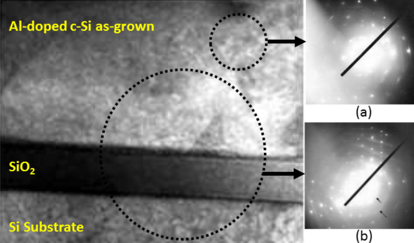
I demonstrated a novel microelectronics semiconductor fabrication process used to produce localized regions of silicon-on-insulator (SOI) including single-crystal, highly p-doped silicon (p-Si) over buried silicon dioxide (SiO2) using a solid metal aluminum (Al) film. At $400^\circ \textrm{C}$, Si is deposited by molecular beam epitaxy and diffuses with an average diffusion length of $\sim1 \mu\textrm{m}$ in solid Al. The diffused silicon grows epitaxially at the buried Al-Si interface, pushing the Al film upward, then grows laterally over regions of oxide (SiO2).
Transmission Electron Microscopy (TEM)
The progressive thin film layers are shown in a transmission electron microscope (TEM) image -- silicon substrate, SiO2, and aluminum-doped single-crystal (c-Si) as-grown during the fabrication process. This process, called solid-metal-mediated epitaxy (SMME), is described in a video created from an original 2001 research group meeting presentation. [video pending]
As shown in the TEM image using electron diffraction, the result is a single crystal Si thin film over the oxide region.
Sample Preparation
Sample polishing
Argon ion milling
[content pending]
Scanning Electron Microscopy (SEM)
[content pending]
Reflective High Energy Electron Diffraction (RHEED)
[content pending]