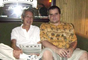
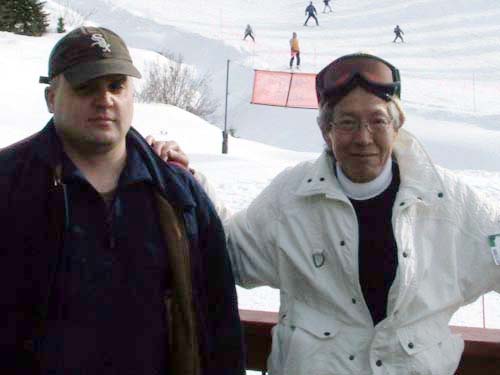
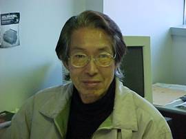
Professor Raphael Tsu (with Tsu replaced by Zhu in pinyin) is a world leader in the areas of quantum properties of materials and device physics. An acknowledged authority in these subjects Professor Tsu has published nearly two hundred scholarly papers in scientific journals; an author of a monograph on quantum wells and superlattice materials and devices [1] of which he is a co-inventor, holder of several patents for his discoveries and invention. The description of his research contributions while at the IBM, T.J. Watson Research Center in Yorktown Heights was presented to the White House by the US Army Research Office, The Superlattice Story, played an important role in the 90s towards the US National Nanoscience Initiative (NNI).
Professor Tsu was born in a Catholic family in Shanghai, China. It is not generally known that the establishment of the Chinese Catholic Church in 1601 by Ricci, a Jesuit, was helped from within the Emperors court of the Ming Dynasty. As a child he was inspired by his great uncle who in 1926 was amongst the first six Chinese bishops ever to be consecrated at the Vatican in Rome and as a teenager by his US educated father Adrian and French educated uncle, Louis. His father side grandfather and great uncle were pioneers in power plant and modern shipyard in Shanghai. When he was leaving Shanghai, his great uncle, in his death bed told him to remember the old Chinese saying that to succeed needs the right tool. Raphael Tsu emigrated to the west, first to study physics in England and later earned a PhD from Ohio State University. Professor Tsu built upon the progress in quantum mechanics made during the first half of the twentieth century into man-made quantum solids.
After several years working as a member of the Technical Staff at the world famous Bell Laboratories (BTL) at Murray Hill, NJ, developing ultrasonic amplifier, a mechanism invented by Dr. D.L. White, Professor Tsu moved to the IBM, T.J. Watson Research Center in Yorktown Heights, NY as an associate to Dr. Leo Esaki, the inventor of Esaki diodes [2] and Physics Nobel laureate in 1973. That was the beginning of his well known collaboration with Esaki, working on the theory of man-made quantum materials, superlattices and quantum wells.
By his theoretical calculations Professor Tsu proved that the quantum states can be designed in multiple layers of semiconductors in a superlattice structure. In comparison to the atomic size lattice constants of natural crystals, the periodic repeat distance in man-made devices can be much longer and hence the relevant reciprocal wave vector and crystal momentum are very small. He also provided the first quantum theoretical calculations of Negative Differential Conductance (NDC) in such artificial materials [3].
Dr. Tsu’s theory required the fabrication of precise multi-layer semiconductor films. Such fabrication can only be achieved with ultra-high purity chemicals, heated to the vapor state and then allowing the vapor to condense on single crystal supporting bases known as substrates, while the entire assembly is held under extremely low gas pressure in very high vacuum. This process is repeated, alternating with vapors of different compositions until a superlattice with the desired thickness and number of atomic layers are produced. The initial rapid development of these new materials and devices [1] owes much to the professional competition between IBM and Bell telephone corporations. These works lead to the discovery of zone-folding in energy-momentum for electrons [3] as well as for phonons [4], resonant tunneling [5,6], the famous Tsu – Esaki current density formula [5,7], and the tunneling time [8]. Returning from a year in Max Planck Institute, Stuttgart, under the Alexander von Humboldt Award, where Professor Tsu served to popularize superlattice and quantum wells in Europe and Germany, he was given a new assignment at IBM, to catch up with BTL in laser annealing, where the most perfect silicon was produced. It was during this phase of his career; he discovered that crystalline silicon may be amorphized by pulsed UV laser, [9] and teaming up with Dr. Jim Van Vecten to propose the non-thermal reordering with high power pulse laser. [10]
Later Professor Tsu joined the Amorphous Semiconductors Institute (ASI) and directed energy research at Energy Conversion Devices (ECD) in MI near Detroit invited by the famous inventor Stan Ovshinsky. His contribution there included the first experimental determination of the volume fraction of crystallinity for conductivity percolation in amorphous silicon and Germanium [11], and providing experimental proof the existence of an intermediate order. [12] He discovered experimentally that post annealing with H2 and even O2 can drastically remove dangling bond defects in amorphous silicon.[13] During 1985-1987 Professor Tsu was the amorphous silicon program group leader at the National Renewable Energy Laboratory (then known as SERI, Solar Energy Research Institute) at Golden, Co. His theoretical derivation of the relationship between the optical absorption and disorder in amorphous silicon and germanium in terms of fundamental constants shows that the slope of the famous Tauc plot is uniquely determined by the oscillator strength of the transition, the deformation potential and the mean deviation of the atomic coordinates obtained from the RDF. [14] Other important theory includes hopping conduction in superlattice [15], and Bloch oscillator [16] which became the highest THz oscillators.
Dr. Tsu is currently holder of the position of Distinguished Professor of electrical engineering at the University of North Carolina at Charlotte. Early on at UNCC, he became the first to offer proof that quantum confinement plays an important role in porous silicon, [17] as well as providing the theory and experiment of a quantum step, instead of quantum well. [18] He teamed up with Prof. E. Nicollian and Q. Ye [19] in the earliest conductance measurements through silicon quantum dots, showing conductance peaks leading conductance steps, a many body effect which is only understood recently. [20] Other recent research interests of his include the theory of dielectric constant, capacitance and doping of a quantum dot [21] [22], [23]. Basically as size is reduced to nanometer regime, dielectric constant is drastically reduced, making doping almost impossible, and the capacitance can only be defined via energy because equal potentials for few electrons are meaningless in general. [24] This work led to extremely curious results, the difference in the total interaction energy of N electrons confined inside a sphere versus N contains features given by the periodic table of elements, the shell model of the atomic system. [25]
He was also amongst the first to derive the quantum mechanical formula to calculate the impedance of a wave function and show that just as Maxwell?s electromagnetic waves experience 376.7 W free space impedance, the propagation of a quantum mechanical wave even in a perfectly phonon free, non-dissipative system involves a quantum wave impedance, QWI ~ Nh/e2, where h is Planck’s constant, e the unit of electronic charge and N is an integer or a fractional number [26].
In 1972, he organized a group and was invited by the Chinese Science Academy which resulted in the first report on the technology in China published in Scientific American. This led to his involvement through establishing the first Chinese Scientific delegation visit to the US, which was invited by the US-China Relations Committee of the US Academy of Science in November. During this visit, he worked with the US State Department for the program and logistics on the East Coast. This effort contributed to the opening of scientific exchange between United States and China.
Professor Raphael Tsu is a fellow of the American Physical Society and member International Advisory Board of the Microelectronic Journal, Elsevier; winner of: Outstanding Contribution Award -IBM 1975; Alexander von Humboldt Award 1975; Co-winner Am. Phys. Soc. International New Materials Prize 1985
Reference
1. Applying the insight into superlattices and quantum wells for nanostructures: Low-dimensional structures and devices, Microelectronics J. 38, no.10-11, p.959-1012 Oct/Nov 2007.
2. New Phenomenon in narrow germanium p-n junctions, Phys. Rev. 109, 603 (1958).??
3. See Twenty years later, after the path breaking work of Esaki and Tsu on negative differential conductivity in superlattices, I realized that I had in fact anticipated their basic physics, albeit in a more primitive form: What was not possible in bulk semiconductors, appeared to become possible in superlattices with their much longer period? Herbert Kroemer in http://nobelprize.org/nobelprizes/physics/laureates/2000/kroemer-autobio.html See also L Esaki and R. Tsu, IBM J. Res. Develop. 14, 61 (1970).
4. Phonon and polariton modes in a superlattice, R. Tsu and S. S. Jha, Appl. Phys. Lett. 20, 16 1972.
5. R. Tsu and L. Esaki, Appl. Phys Lett. 22, 562 (1973).
6. Resonant Tunneling in Semiconductor Double Barriers. L.L. Chang, L. Esaki and R. Tsu, Appl. Phys. Lett. 24, 593 (1974).
7. Quantum-mechanical tunneling time and its relation to the Tsu-Esaki formula, Marc M. Cahay , et al Proceedings of SPIE 1675, 142 (1992).
8. Superlattice to Nanoelectronics, R. Tsu, (Elsevier 2005) Chapter 2.
9. Order-Disorder Transition in Single-Crystal Silicon by Pulsed UV Laser, R. Tsu, R. T. Hodgson, T. Y. Tan and J. E. Baglin, Phys. Rev. Lett.? 42, 1356 (1979).
10. Nonthermal Pulsed Laser Annealing of Si; Plasma Annealing, J. A. Van Vechten, R. Tsu and? F. W. Saris, Phys. Lett. 74A(6), 422 (1979).
11. Critical Volume Fraction of Crystallinity for Conductivity Percolation in P-doped Si:F:H Alloys, R. Tsu, J. G. Hernandez, S. S. Chao, S. C. Lee and K. Tanaka, APL 40, 534 (1982).
12. Electroreflectance and Raman Investigation of Glow-Discharge Amorphous Si:F:H, R. Tsu, M. Isu, S. R. Ovshinsky and F. H. Pollak, Solid State Comm. 36, 817 (1980).
13. Passivation of Dangling Bonds in Amorphous Silicon and Germanium by Gas Absorption, R. Tsu, D. Martin, J. Hernandez and S. R. Ovshinsky, Phys. Rev. B 35,2385 (1987).
14. Optical Absorption and Disorder in Hydrogenated amorphous Si-Ge and Si-C Alloys systems, R. Tsu, P. Menna, and A.H. Mahan, Solar Cells, 21 189,(1987)
15. Hopping Conduction in a Superlattice, R. Tsu, and G. Dohler, Phys. Rev. B 12, 680, (1975).
16. Stark Quantization in? Superlattices, R. Tsu and L. Esaki, Phys. Rev. B 43, 5204 (1991).
17. Correlation of Raman and? PL Spectra of Porous Silcon, R. Tsu, H. Shen and M. Dutta, Appl. Phys. Lett. 60, 112 (1992).
18. Optical Properties of Quantum Steps, H. Shen, F. H. Pollak and R. Tsu, Appl. Phys. Lett.57,13(1990).
19. Resonant Tunneling Via Microcrystalline Silicon Quantum Confinement, Q. Y. Ye, R. Tsu and E. H. Nicollian, Phys. Rev. B 44, 1806 (1991).
20. Revisiting tunneling via Si-quantum dots, R. Tsu, Microelectr. J.,2007, in press, doi:10.1016/j.mejo.2007.07.008.
21. A Simple Model For The Dielectric Constant Of Nanoscale Silicon Particle, R. Tsu, D.Babic, and L.Ioriatti,J. Appl. Phys. 82, 1327(1997)
22. Ground State Energies of One-and Two-Electron Silicon Dots,D. Babic, R. Tsu and R. F. Greene, Phys. Rev. B 45, 14150 (1992).
23. Doping of a Quantum Dot, R. Tsu and D. Babic, Appl. Phys. Lett. 64, 1806 (1994).
24. Classical capacitance of few-electron dielectric spheres, J. Zhu, T.J. LaFave and R. Tsu, Microelectronic J. 37, 1293 (2006)
25. Capacitance: A property of nanoscale materials based on spatial symmetry of discrete electrons, T. LaFave Jr., and R. Tsu, Microelectronics J. 38 11-12, 200726. Timir Datta & Raphael Tsu arXiv:cond-mat/0311479v1


